


If you were to open up your laptop, you would find a central processor whose job is effectively set in stone at the factory. It runs software, but the hardware itself—the physical pathways that electrons travel—never changes. However, there is a class of chips that breaks this rule: the Field-Programmable Gate Array, or FPGA. Think of these as “blank slate” microchips. Engineers can write code to physically rewire the chip’s internal circuitry to perform specific tasks with incredible speed and efficiency, and then “reprogram” them later if requirements change. While they rarely make headlines in the consumer world, FPGAs are the invisible engines inside MRI machines, 5G towers, and professional broadcast cameras. Today, AMD is updating one of the most vital families in this space with the launch of the Kintex UltraScale+ Gen 2.
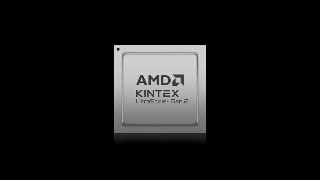
This new release isn’t about reinventing the wheel but rather modernizing a critical workhorse. The Kintex line has long sat in the “mid-range”—the sweet spot between massive, power-hungry data centre chips and tiny, low-power sensors. With the Gen 2 update, AMD is injecting this established platform with the specific technologies needed for the next decade of edge computing and industrial automation.
Solving the Bandwidth Bottleneck
For modern embedded systems, the bottleneck is rarely raw processing power; it is moving data. Whether it is an 8K video stream or real-time telemetry from an industrial robot, getting information in and out of the chip is usually where performance stalls. AMD has addressed this head-on with a massive jump in capability, claiming up to a five-fold increase in memory bandwidth compared to the previous generation. This is driven by a new integrated memory subsystem that supports modern LPDDR4X, LPDDR5, and LPDDR5X standards.
For developers, this inclusion effectively removes the speed limit. Previous mid-range FPGAs often choked when trying to shuttle data between the logic gates and external memory, forcing engineers to compromise on resolution or data fidelity. The inclusion of up to six hard memory controllers ensures that data-heavy tasks like real-time video processing can run smoothly without bottlenecks. This is a significant quality-of-life improvement for system architects who have previously had to resort to complex, power-hungry workarounds to achieve similar throughput.
Connectivity for the Professional
On the connectivity front, the Gen 2 family introduces PCIe Gen 4 support. While the computing world is already flirting with Gen 5, Gen 4 remains the practical standard for the mid-range market, offering a substantial bandwidth increase over previous devices. This is particularly critical for “AV-over-IP” applications, where professional broadcasters need to move uncompressed 4K and 8K video signals across networks with zero dropped frames. By providing native support for these speeds, AMD is allowing broadcast equipment manufacturers to build smaller, cooler-running devices that don’t skimp on signal integrity.
The new family is comprised of three key devices: the 2KU030P, 2KU040P, and 2KU050P. These chips offer a logic density ranging from 328K to 491K System Logic Cells, providing ample room for complex circuit designs. For signal processing tasks, such as ultrasound beamforming in medical devices, the devices pack up to 1,872 DSP slices. Connectivity is further handled by up to 24 GTY transceivers capable of speeds reaching 32.75 Gb/s, alongside a massive count of up to 396 high-performance I/O pins that support standards like MIPI D-PHY for direct connection to camera sensors.
A Security Overhaul for the Quantum Age
One of the most forward-thinking aspects of this announcement is the focus on long-term security. We are entering an era where “harvest now, decrypt later” attacks are a genuine concern. This is a scenario where bad actors steal encrypted data today, storing it with the intention of cracking it years down the road once quantum computers become powerful enough to break current encryption standards. To counter this, the Kintex UltraScale+ Gen 2 is built with Post-Quantum Cryptography (PQC) support and is CNSA 2.0 capable.
It features a dedicated security engine that handles encryption and authentication, protecting not just the data flowing through the chip, but the integrity of the hardware itself. This engine manages the bitstream—the code that defines the FPGA’s personality—ensuring that it cannot be cloned or tampered with. For industries like healthcare and aerospace, where equipment is deployed for decades, having built-in defenses against future threats is a major necessity.
Built for the Long Haul
Perhaps the most reassuring spec for enterprise customers is not a speed or a feed, but a date. AMD is making a very specific promise regarding longevity with this release: these chips will be available until at least 2045. In a consumer tech industry where a phone is considered obsolete in three years, a 20-year lifecycle is staggering. However, for a medical company building a new diagnostic machine or an industrial firm designing a robotic assembly line, this stability is invaluable. Regulatory approvals for medical devices can take years; once a design is certified, changing a single chip can trigger a costly re-certification process. This long lifecycle commitment means engineers can design a system today and know they will still be able to source replacement parts two decades from now without redesigning their entire motherboard.
Availability
Design teams can start working immediately, as documentation is available now and support is already integrated into the latest versions of the Vivado and Vitis design tools. However, physical implementation will take a bit longer. Silicon samples are expected to ship in the fourth quarter of 2026, with full production planned for the first half of 2027. Evaluation kits will also start sampling in late 2026, allowing developers to begin testing their designs on real hardware before mass manufacturing begins.