Tag Archives: SEM

Macnica Inc. Selected Leading Innovation Consultancy Orangeleaf Consulting in Malaysia to Propel Accelerated Digital Transformation Excellence in Japan

KUALA LUMPUR, Malaysia, Dec. 29, 2023 /PRNewswire/ — Macnica Inc. headquartered at Yokohama City, Kanagawa Prefecture, President: Kazumasa Hara, hereinafter referred to as “Macnica” is pleased to announce a strategic collaboration with Orangeleaf Consulting, CEO, Ellice Ng Pui San, a renowned digital transformation consultancy in Malaysia. The collaboration aims to strengthen Enterprise Digital Transformation (DX) capabilities and drive innovation within the Japanese manufacturing market. Orangeleaf Consulting brings a wealth of experience in guiding global organizations through successful digital transformations, with a proven track record of implementing cutting-edge technologies and strategies in the global market.

Macnica Inc. Selected Leading Innovation Consultancy Orangeleaf Consulting in Malaysia to Propel Accelerated Digital Transformation Excellence in Japan

At Orangeleaf Consulting, helmed by visionary, Ellice Ng, “We are honored to collaborate with Macnica, a leader in the technology solutions space in Japan. Together, we look forward to driving meaningful digital transformation outcomes and contributing to the success of Macnica’s clients in the manufacturing industry. We aim not just to influence, but to revolutionize the way people think and act in the enterprise software industry through advance technology. Our ultimate aspiration: Operate dynamically, pushing boundaries to achieve audacious goals, instilling a culture of relentless innovation and unparalleled success.”

In addition, Ellice also mentioned the manufacturing industry is a significant and integral part of Japan’s economy. Japan has long been recognized as a major global player in manufacturing, particularly in sectors such as automotive, electronics, machinery, and precision equipment.

Problem Statement: Why is Digital Transformation (DX) in Japan’s manufacturing industry not progressing? The challenge is to cultivate DX culture and develop human resources.
The wave of Industry 4.0 (Fourth Industrial Revolution), which was born in Germany in 2011, greatly shook the manufacturing industry in Japan. Many companies in Japan have been calling for “DX (digital transformation) in the manufacturing industry and have set up DX promotion departments and managers to make investments. DX is a strategic initiative that involves the adoption and integration of digital technologies to drive organizational growth, improve operations, and deliver enhanced value to customers.

However, many companies face obstacles in cultivating a DX culture and developing human resources for effective implementation. The lack of alignment in mindset and culture between top management and business departments is identified as a major internal barrier. A true DX requires in-house capabilities, highlighting the importance of developing internal leaders who can design business processes across departments. Macnica, a key player in the DX field aim to advocate for the use of the latest technology platform low-code tools to involve individuals without coding knowledge in projects, fostering collaboration between business and IT departments.

Digital Transformation (DX) team is crucial in the modern business landscape to enhance business processes, improve efficiency, and foster innovation.
Macnica’s vision focuses on an “experience-first” approach, encouraging trial and error to address challenges in manufacturing sites. The company believes that in-house initiatives are crucial for the success of DX, allowing for greater speed, flexibility, and response to site-specific needs. Macnica recently introduced its Digital Synergy Factory-low-code development support service as a means to materialize its vision and accelerate manufacturing DX support services. The company has also welcomed a knowledgeable partner to further enhance its efforts in this domain.

Macnica’s decision to collaborates with its partner, Orangeleaf from Malaysia – the leading low-code expert, to provide comprehensive Digital Transformation (DX) consulting using low-code technology. Having successfully implemented over 100 DX projects in manufacturing, insurance, and retail across Europe, Singapore, and Malaysia, Orangeleaf Consulting focus is on empowering clients to drive their DX initiatives without lock-in contract. The support spans from long-term planning to agile application development, including information on cutting-edge technologies. Macnica and Orangeleaf aim to contribute to the advancement of DX in the Japanese manufacturing industry by leveraging best practices and offering holistic assistance in consulting, human resource development, and organizational building.

Orangeleaf impressed the “experience-first” using low-code tools with Macnica Employees 
Macnica had a challenge in their semiconductor business – it used to take 15 minutes for sales people to set delivery dates for certain customers using a mix of data from ERP and Excel. To solve this, Macnica teamed up with Orangeleaf to create a simple app using low-code technology. The amazing part? The whole process, from planning to using the improved system, only took 14 hours! Now, instead of 15 minutes each time, they get things done in just seconds. It worked so well that now more ideas for improving their business keep popping up.


About Macnica’s Smart Manufacturing Business
Macnica is also involved in DX support for the manufacturing industry based on the technological capabilities it has cultivated as a semiconductor trading company and its experience in implementing cutting-edge technologies such as AI and IoT. In the future, as DX accelerates in the manufacturing industry, security issues will also emerge. Macnica has also introduced the world’s most advanced technology in the field of security to Japan. Japan’s manufacturing industry faces a unique set of challenges. Macnica will strive to create new business opportunities and develop society by discovering issues together and promoting DX while staying close to customers’ concerns. 

About Orangeleaf Consulting 
Orangeleaf Consulting, a trailblazing digital transformation consultancy headquartered in Malaysia, stands at the forefront of empowering organizations to embrace innovation and navigate the evolving landscape of technology. With a commitment to driving impactful change, Orangeleaf specializes in advance technology such as low-code solutions, offering a swift and effective approach to application development and process improvement.

Orangeleaf Consulting believes in more than just technological solutions; we strive to instigate meaningful cultural shifts within organizations, fostering innovation and paving the way for sustainable success.

About us: www.orangeleaf.com.my

About Macnica Inc
Macnica is a service/solution company that handles the latest technologies in a comprehensive manner, centered on semiconductors and cyber security. Developing business in 81 locations in 23 countries/regions around the world, leveraging the technological capabilities and global network cultivated over a history of more than 50 years, we discover, propose, and implement cutting-edge technologies such as AI, IoT, and autonomous driving.

Please visit: www.macnica.co.jp 

EV Group Brings Revolutionary Layer Transfer Technology to High-Volume Manufacturing with EVG®850 NanoCleave™ System


Infrared laser cleave technology enables ultra-thin-layer transfer from silicon substrates with nanometer precision, revolutionizing 3D integration for advanced packaging and transistor scaling

ST. FLORIAN, Austria, Dec. 8, 2023 /PRNewswire/ — EV Group (EVG), a leading supplier of wafer bonding and lithography equipment for the MEMS, nanotechnology and semiconductor markets, today introduced the EVG®850 NanoCleave™ layer release system—the first product platform to feature EVG’s revolutionary NanoCleave technology. The EVG850 NanoCleave system enables nanometer-precision release of bonded, deposited or grown layers from silicon carrier substrates using an infrared (IR) laser coupled with specially formulated inorganic release materials in a proven, high-volume-manufacturing (HVM) capable platform. As a result, the EVG850 NanoCleave eliminates the need for glass carriers—enabling ultra-thin chiplet stacking for advanced packaging, as well as ultra-thin 3D layer stacking for front-end processing, including advanced logic, memory and power device formation, to support future 3D integration roadmaps. 

View inside the EVG®850 NanoCleave™ layer release system, with the pre-processing module bay and the mechanical release module in the background. Source: EV Group.

The first EVG850 NanoCleave systems have already been installed at customer facilities, and nearly two dozen product demonstrations are underway with customers and partners at customer sites and EVG’s headquarters.

Silicon Carriers Benefit 3D Stacking and Back-end Processing 
In 3D integration, glass substrates have become an established method for building up device layers through temporary bonding with organic adhesives, using an ultraviolet (UV) wavelength laser to dissolve the adhesives and release the device layers, which are subsequently permanently bonded onto the final product wafer. However, glass substrates are difficult to process with semiconductor fab equipment that have been designed primarily around silicon, and that require costly upgrades to enable glass substrate processing. In addition, organic adhesives are generally limited to processing temperatures below 300 °C,  limiting their use to back-end processing.

Enabling silicon carriers with inorganic release layers avoids these temperature and glass carrier compatibility issues. In addition, the nanometer precision of IR laser-initiated cleaving allows for processing extremely thin device wafers without changing processes of record. Subsequent stacking of such thin device layers enables higher-bandwidth interconnects and new opportunities to design and segment dies for next-generation, high-performance devices.

Next-generation Transistor Nodes Require Thin-layer Transfer Processes
At the same time, transistor roadmaps for the sub-3-nm node call for new architectures and design innovations such as buried power rails, backside power delivery networks, complementary field-effect transistors (CFETs) and 2D atomic channels, all of which require layer transfer of extremely thin materials. Silicon carriers and inorganic release layers support process cleanliness, material compatibility and high processing temperature requirements for front-end manufacturing flows. However, until now, silicon carriers had to be completely removed using grinding, polishing and etching processes, which results in micron-range variations across the surface of the working device layer, making this method unsuitable for thin-layer stacking at advanced nodes.

“Releasable” Fusion Bonding
The EVG850 NanoCleave utilizes an IR laser and inorganic release materials to enable laser cleaving from silicon carriers with nanometer precision in production environments. The innovative process eliminates the need for glass substrates and organic adhesives, enabling front-end process compatibility for ultra-thin-layer transfer and downstream processes. The most demanding front-end processing is supported by the EVG850 NanoCleave’s high-temperature compatibility (up to 1000 °C) while the room-temperature IR cleaving step ensures device layer and carrier substrate integrity. The layer transfer process also eliminates the need for expensive solvents associated with carrier wafer grinding, polishing and etching.

The EVG850 NanoCleave is based on the same platform as EVG’s industry-leading EVG850 series of automated temporary bonding/debonding and silicon-on-insulator (SOI) bonding systems, with a compact design and HVM-proven wafer handling system.

According to Dr. Bernd Thallner, corporate R&D project manager at EV Group, “Since EVG’s founding more than 40 years ago, our vision has been steadfast in being the first in exploring new techniques and serving next-generation applications of micro- and nanofabrication technologies. Recently, 3D and heterogeneous integration have stepped into the spotlight as key drivers of performance improvements on new semiconductor device generations. This in turn has brought wafer bonding front and center as a critical process for continuing PPACt (power, performance, area, cost and time-to-market) scaling. With our new EVG850 NanoCleave system, EVG has merged the benefits of temporary bonding and fusion bonding into one versatile platform supporting our customers’ ability to extend their future roadmaps in both advanced packaging and next-generation scaled transistor design and manufacturing.”

For more information on the EVG850 NanoCleave layer release system, visit https://www.evgroup.com/products/bonding/temporary-bonding-and-debonding-systems/evg850-nanocleave.  

About EV Group (EVG)
EV Group (EVG) is a leading supplier of equipment and process solutions for the manufacture of semiconductors, microelectromechanical systems (MEMS), compound semiconductors, power devices and nanotechnology devices. Key products include wafer bonding, thin-wafer processing, lithography/nanoimprint lithography (NIL) and metrology equipment, as well as photoresist coaters, cleaners and inspection systems. Founded in 1980, EV Group services and supports an elaborate network of global customers and partners all over the world. More information about EVG is available at www.EVGroup.com.

Contacts:   

Clemens Schütte

David Moreno

Director, Marketing and Communications

Principal

EV Group

Open Sky Communications

Tel: +43 7712 5311 0

Tel: +1.415.519.3915

E-mail: Marketing@EVGroup.com

E-mail: dmoreno@openskypr.com  

Photo – https://techent.tv/wp-content/uploads/2023/12/ev-group-brings-revolutionary-layer-transfer-technology-to-high-volume-manufacturing-with-evg850-nanocleave-system.jpg
Logo – https://techent.tv/wp-content/uploads/2023/12/ev-group-brings-revolutionary-layer-transfer-technology-to-high-volume-manufacturing-with-evg850-nanocleave-system-1.jpg

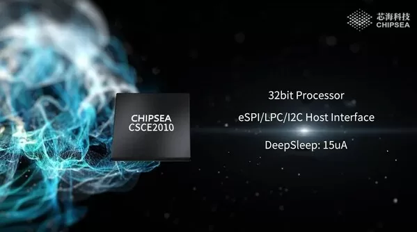
Chipsea Technologies (Shenzhen) Co., Ltd., a “new player” in the global PC industry chain, has once again been awarded an Intel Platform Component List (PCL) certification, for its new EC product E2010

SHENZHEN, China, Nov. 25, 2023 /PRNewswire/ — Recently, China’s A-share listed company Chipsea Technologies (stock code: 688595) has seen its new generation EC chip CSCE2010 successfully passed Intel PCL (Platform Component List) certification, turning it into the world’s first EC product to meet the advanced process requirements of Intel MTL. Over the past two years, Chipsea Technologies has successively launched two 32-bit high-performance EC chips, namely the product CSC2E101 (E2101) for the commercial PC market and the product CSCE2010 for the consumer PC market. Both of them have met Intel PCL certification, fully demonstrating the company’s rich technological accumulation and strong innovation power in EC field, and have achieved the company’s breakthroughs both in technology and business circles. Chipsea Technologies is rapidly establishing itself as a dynamic and innovative force in the global PC industry. Through a series of forward-looking product innovations, the company has kicked off multiple products such as EC, PD, USB Hub, HapticPad® solutions, and BMS (battery management system), and signed a cooperation memorandum and established a good cooperative relationship with Intel. Looking  ahead, Chipsea is planning to build a global supply system to provide global and diversified supply guarantees and offer customers with more competitive products.

Established 20 years ago, Chipsea Technologies is an integrated circuit design company that integrates sensing, computing, control and connection. The company has rich technical accumulation in the fields of analog signal chain and MCU (microprogrammed control unit), and has become a global leader in the fields of pressure touch and health measurement chips. The company debuted on China’s A-share market in 2020, and has become “China’s first stock in the field of signal chain chip.”

new EC product E2010

Currently, Chipsea Technologies is on a fast development track, with its products and businesses spanning multiple market segments such as automotive electronics, computers and communications, BMS (battery management system), industrial measurement and control, health measurement, and AIoT (AI + IoT). Meanwhile, Chipsea Technologies has built a total quality management (TQM) system that can meet international standards such as ISO9001, GB/T29490, ISO27001, ISO26262, IATF16949, covering the full-lifecycle quality management of products from chip definition to design, through manufacturing and package testing, to final mass production and delivery, to ensure high reliability, high performance and high quality of products, and bring more novel ideas and surprising experiences to customers around the world. Chipsea’s commitment to reliability, performance, and quality not only meets but exceeds global benchmarks, fostering innovative and enriching experiences for customers worldwide.

Contact: sales@chipsea.com; lutt@chipsea.com 

www.chipsea.com

Source: Chipsea Technologies (Shenzhen) Corp.

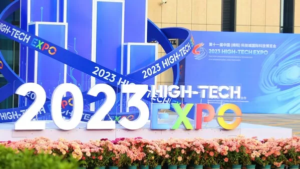
Chengdu showcases technological strength at high-tech expo

CHENGDU, China, Nov. 24, 2023 /PRNewswire/ — Chengdu, capital of Southwest China’s Sichuan province, demonstrated its strength in sci-tech innovation at the 11th China (Mianyang) Science and Technology City International High-Tech Expo, which kicked off on Wednesday in Mianyang, Sichuan province.

Chengdu showcases technological strength at the 11th China (Mianyang) Science and Technology City International High-Tech Expo.

Co-sponsored by the Ministry of Science and Technology and the Sichuan provincial government, the expo covers a total exhibition area of 40,000 square meters, with over 300 participating companies and more than 3,000 exhibits.

Scientific research institutions and innovative enterprises based in Chengdu brought over 30 leading technological achievements to this year’s expo, according to Chengdu science and technology bureau.

Zou Sifei, a staff member of the Tianfu Xinglong Lake Laboratory, one of the key laboratories under Sichuan’s Tianfu Laboratories plan, said his laboratory has conducted in-depth research into revolutionary optoelectronic materials, optoelectronic devices and optoelectronic systems, and has been promoting the transformation of its research achievements.

The laboratory displayed its latest achievements in scientific research transformation at the expo in fields including information metamaterials and wireless communication, material photonics, and advanced optical devices, he said.

He Weizhi, an executive at Tsinghua Sichuan Energy Internet Research Institute, said the institute holds more than 560 invention patents and is facilitating the transformation of technological achievements to empower regional economic development.

The institute demonstrated a number of products which have been transformed from its technological achievements, including a “Floating-Crawling” dual-mode underwater inspection robot and a miniature intelligent electric current sensor.

“In addition to showcasing our technological prowess at the expo, we also hope to attract more versatile talents to join our institute for further studies,” he said.

Xu Huawei, an executive at Sichuan Tengden Sci-tech Innovation Co Ltd, said the expo showcases cutting-edge achievements from home and abroad, creating a plethora of growth prospects and collaborative opportunities to the company.

As a leading player in Chengdu in the field of industrial UAV, Tengden displayed the models of its self-developed UAVs, which can be widely used in fields including artificial rainmaking, emergency communication and forest fire inspection, Xu said.

Shi Da, sales engineer of Chengdu Jiujin Technologies Co Ltd, whose products are used in fields such as antenna testing, wireless communication and aerospace, said the expo gathers professionals from various industries, creating a perfect chance to promote the company’s image and products and to facilitate communication with partners.

DEEPX Honored with Three CES Innovation Awards 2024 for Leading-Edge AI Chip Tech

Korean fabless startup unleashes world’s most innovative AI chip technology — ultra-gap source technology

– DEEPX is honored with three CES Innovation Awards 2024 in its core focus areas: Computer Hardware, Embedded Technology, and Robotics.
– The brand is a fabless AI chipmaker with world-leading innovation in cutting-edge source technologies — specifically ultra-gap source technology.

SEOUL, South Korea and LAS VEGAS, Nov. 17, 2023 /PRNewswire/ — DEEPX (CEO, Lokwon Kim), an AI chipmaking startup, is announcing that its proprietary ultra-gap source technology for AI chips has been recognized with three CES Innovation Awards 2024 — in Computer Hardware, Embedded Technology, and Robotics — ahead of the January 2024 CES trade show in Las Vegas, Nevada.

Join DEEPX at Booth #9069, North Hall during CES 2024 to experience the latest in AI chip technology and explore DEEPX’s Early Access Customer Program. 

DEEPX’s All-in-4 AI Total Solution, DX-H1, and DXM1 are honored with CES Innovation Awards 2024.

As the world’s largest electronics exhibition since 1967, CES’ Innovation Awards, organized by the Consumer Technology Association (CTA), have served as a global beacon for technological innovation. DEEPX is the first AI chip company in the world to be honored with CES Innovation Awards in all three categories, and the brand anticipates that the positive recognition from these awards will soon be shared more broadly, through expanding international partnerships and attracting further investment.

The following DEEPX solutions were recognized: 

  • Embedded Technology category: An “All-in-4 AI Total Solution” consisting of four AI chips optimized for AI capabilities and performance that can be applied to various embedded systems
  • Computer Hardware category: The DX-H1, a technology specialized in minimizing energy consumption in high-performance AI computation processing in servers and data centers to reduce carbon emissions
  • Robotics category: The DX-M1 module, which innovatively realizes the intelligentization of edge devices such as robots for unmanned industrial sites and social infrastructure as well as daily life

Each of these solutions utilizes DEEPX’s ultra-gap source technology, its core and independently developed technology. The brand’s AI chip source solutions offer the latest AI algorithm support technology for edge AI applications, GPU-level high AI accuracy, and the world’s highest effective power-to-performance ratio. DEEPX is also the only AI chip company in the world to offer: an All-in-4 AI Total Solution consisting of four products optimized for various AI applications; technology that minimizes on-chip SRAM and off-chip DRAM usage requirements to minimize AI technology implementation costs; and DEEPX Software Development Environment (DXNNTM) technology that can unify and support four AI chip products for development of various AI applications. In addition, DEEPX is actively honing the cutting edge of AI chip technology and striving to lead the way — it currently has over 200 patents pending in the U.S., China, and Korea, the most in the world for edge AI chip development.

“DEEPX set out from the start to dominate the global market by developing the world’s best AI chip source technology, and, through hard work and dynamic innovation, we have already set the standard for AI chip technology,” remarked DEEPX CEO Lokwon Kim. “The fact that the first solution we developed — ultra-gap source technology — has been recognized with three CES Innovation Awards is an immense honor and a truly promising start. As we move forward, we will continue to challenge ourselves to constantly develop new technologies so that the name ‘DEEPX’ will be synonymous with ‘the world’s best original technology company’.”

DEEPX will showcase the winning source technologies and more at Booth #9069, North Hall during CES 2024, January 9-12, 2024, in Las Vegas, NV, as it leads the way in shaping the future with innovation.

<ABOUT DEEPX>
Founded in anticipation of an era when artificial intelligence will be as ubiquitous as electricity and Wi-Fi, DEEPX develops the underlying technology for high-performance AI chips and computing solutions that can make all electronic devices intelligent. DEEPX’s AI chips are optimized for various AI applications, improving the energy efficiency of AI devices and enabling efficient AI functions. Currently, DEEPX is cooperating with customers such as Hyundai Kia Motors Robotics LAB, POSCO DX, and Jahwa Electronics, which signed a mass production cooperation agreement earlier this year. The brand is also expanding cooperation with more than 30 global companies in smart cameras, control and security systems, robots, AI medical devices, and AI servers, while it scales up business globally, especially in the United States, China, and Taiwan region.

For more information, please visit: https://deepx.ai/

ERS electronic introduces “High Power Dissipation” Thermal Chuck System, which can dissipate up to 2.5kW at -40°C for Embedded Processors, DRAM and NAND wafer test


MUNICH, Nov. 14, 2023 /PRNewswire/ — ERS electronic, the industry leader in the market of thermal management solutions for semiconductor manufacturing, is introducing its latest “High Power Dissipation” Thermal Chuck System. The technology enables accurate and powerful temperature control of a DUT while performing tests of high-end CPUs, GPUs, and high parallelism DRAM devices in the temperature range between -60°C and +200°C.

High Power Dissipation” is the newest thermal chuck system from ERS electronic, suited for wafer test of complex processors and DRAM and NAND devices.

During temperature wafer probing of complex embedded processors, such as CPUs and GPUs for machine learning, artificial intelligence or data centers, and high parallelism tests, like DRAM and NAND, a very large amount of power needs to be dissipated to avoid overheating. ERS’s new “High Power Dissipation” System can dissipate wattage up to 2.5kW at -40°C on a 300 mm chuck, thereby allowing the testing of single dies as well as tests with full wafer contact. As an added option, the system comes with an industry-best temperature uniformity of ±0.2°C at -40°C, going down to even ±0.1°C between -20°C and +85°C, making it ideal for the testing of sensors.

The thermal chuck consists of several sections that can be controlled individually, thanks to ERS’s patented PowerSense software. When power is applied to the wafer, it immediately detects the increasing heat and reacts quickly by cooling down the affected area.
To achieve the lightning-fast dissipation coupled with the high temperature uniformity, ERS’s new thermal chuck system comes with a chiller cooled with liquid instead of air.

“For the “High Power Dissipation” system, we made a conscious decision to use engineered fluids, as they allow us to meet the dissipation requirements of the targeted applications. For all other major wafer test operations, we continue to favor air as a coolant,” says Klemens Reitinger, CTO of ERS electronic. “What sets our solution apart is not only the exceptional dissipation performance at cold temperatures, but also that it can be combined with an unparalleled temperature uniformity of ±0.1°C. We are working on additional features for this system, which will improve dissipation performance and section monitoring even further, thereby allowing a full dynamic control.”

“ERS’s “High Power Dissipation” thermal chuck system is solving a significant issue that occurs during the testing of high-end processors and DRAM & NAND devices,” says Liang Wang, Vice President of Shanghai Jinni. “As the demand for these IC’s continue to grow, we expect a strong interest for this system from our Chinese customers, which is why we already have it installed here in our common lab with ERS in Shanghai for customer evaluations and demonstrations.”

The High Power Dissipation Chuck System is available to order now.

About ERS:

ERS electronic GmbH has been providing innovative thermal test solutions for the semiconductor industry for more than 50 years. The company has gained an outstanding reputation with its fast and accurate air cool-based thermal chuck systems for wafer probing and its thermal debonding and warpage adjustment tools for FOWLP/PLP.

www.ers-gmbh.com

VisIC Technologies Revolutionizes Automotive Power Electronics with V22TG D3GAN in Advanced Top Side Cooled Isolated Package


NESS ZIONA, Israel, Nov. 14, 2023 /PRNewswire/ — VisIC Technologies Ltd, a global leader in advanced GaN power electronics solutions, is excited to introduce the highly anticipated V22TG D3GAN power package. This revolutionary power package, housed in an advanced gull wing leaded top side cooled isolated package, sets new standards for performance, reliability, and versatility in the automotive industry.

VisIC's V22TG D3GAN Advanced Top-Side Cooled Isolated Package
VisIC’s V22TG D3GAN Advanced Top-Side Cooled Isolated Package

Designed with the future of electric vehicles in mind, the V22TG D3GAN brings together an array of cutting-edge features to deliver exceptional power density and efficiency. This compact power package with a small footprint of 19.7×13.6mm (including leads), provides automotive manufacturers with flexibility in system design and integration. Targeted for automotive AEC-Q101 standard, it can be used as well in the highly reliable field of server power supplies, data centers, solar inverters, and a wide range of industrial applications.

Key Features and Benefits:

1. Advanced Leaded Top-Side Cooled Isolated Package: The V22TG D3GAN is encased in an innovative leaded top-side cooled isolated package. This design promotes excellent thermal management, ensuring optimal performance and reliability in demanding automotive environments. Moreover, the isolated package enhanced the ease of assembly due to no additional isolation needed.

2. Automotive and High Voltage Capability: The V22TG D3GAN is rigorously tested targeting to meet automotive industry standards, making it suitable for a wide range of automotive applications, like OBC, Fuel Cell, and hybrid electric vehicles. With a voltage capability of 650V, this SMD power package can handle high-voltage requirements with effortless efficiency.

3. High Power Density and Low On-Resistance: Offering a low on-resistance of 22mΩ, the V22TG D3GAN delivers outstanding power density, empowering automotive manufacturers to create more compact and lightweight systems without compromising performance. This exceptional power density ensures maximum efficiency and reduced energy losses.

4. Versatile and Easy to Implement: The V22TG D3GAN is designed to support various system configurations, including paralleling of devices, full-bridge, half-bridge topologies, and power factor correction (PFC) circuits. This flexibility allows for seamless integration into a wide array of power electronics applications.

Availability and Sample Shipment:

VisIC Technologies is pleased to announce that samples of the V22TG D3GAN will be available in the first quarter of 2024. This early availability allows manufacturers to assess and experience the performance and benefits of the package firsthand, aiding in the rapid development of the next generation of systems.

“We are thrilled to introduce the V22TG D3GAN power package, which represents a significant breakthrough in automotive power electronics,” said Dr. Tamara Baksht, CEO and Co-Founder of VisIC Technologies Ltd. “This advanced power package not only offers exceptional performance and reliability but also provides the versatility and ease of implementation required for emerging automotive and industrial applications. We are confident that the V22TG D3GAN will empower manufacturers to accelerate the adoption of electric vehicles.”

About VisIC Technologies Ltd:

VisIC Technologies is a world leader in GaN electronics for EV applications, focused on high-power automotive solutions. Its efficient and scalable products are based on deep technological knowledge of gallium-nitride and decades of experience. VisIC Technologies is committed to providing a step function improvement in size and cost of energy conversion systems and is dedicated to high-quality customer support at all development phases. VisIC offers high-power transistor products based upon compound semiconductor Gallium Nitride (GaN) material, aiming to provide products for cost-effective and high-performance automotive inverter systems.

Press contact

Ortal Zanzuri
CFO
VisIC Technologies Ltd.
zanzuri.ortal@visic-tech.com

ICZOOM Named Outstanding e-Commerce Platform of the Year at Prestigious Global IC & Component Exhibition and Conference, IIC Shenzhen 2023; Company Also Wins Global Electronic Component Distributor Excellence Award


HONG KONG, Nov. 9, 2023 /PRNewswire/ — ICZOOM Group Inc. (Nasdaq: IZM) (the “Company” or “ICZOOM”), a B2B electronic component products e-commerce platform, announced today that the Company was named Outstanding e-Commerce Platform of the Year at the prestigious Global IC & Component Exhibition and Conference, IIC Shenzhen 2023. This marks the seventh consecutive year the Company has been named Outstanding e-Commerce Platform of the Year by the major global IC and component exhibition and conference. Separately, the Company’s subsidiary Hjet Supply Chain won top honors with the important Global Electronic Component Distributor Excellence Award.

ICZOOM’s CEO, Mr. Lei Xia commented, “We are honored to be named Outstanding e-Commerce Platform of the Year and to receive the Global Electronic Component Distributor Excellence Award from the prestigious IIC Shenzhen. This is in recognition of our entire team’s hard work and dedication to providing our customers with increased efficiencies, broader and faster access to the components they need, and pricing transparency. This important industry-wide recognition underscores our leadership and unwavering commitment to further success as we continue to meet the needs of our customers and build value for our shareholders.”

IIC Shenzhen 2023 combines industry exchanges, multi-channel interaction, and resources aggregation, and brings together annual innovative product display, technology exchange, high-end forum, and industry summit. The exhibition sets up high-end exhibition areas such as IC design and application area, distributor area, and semiconductor comprehensive exhibition area, etc., to display IC design, EDA\IP, Internet of Things, AI, automotive electronics, green energy, smart industry, wireless technology, and other major emerging technologies and products. For more information please visit https://iic.eet-china.com/index_en.html.

At this year’s event, experts from upstream and downstream enterprises from across leading semiconductor OEMs, distributors, solution providers, and terminal factories (EMS/OEM/ODM) focused on supply chain security issues, elaborated on innovative thinking and insight into market trends, and deeply interpreted supply chain development trends and opportunities under semiconductor cycle variables.

About ICZOOM Group Inc.

ICZOOM Group Inc. (Nasdaq: IZM) is primarily engaged in sales of electronic component products to customers in Hong Kong and mainland China through its B2B e-commerce platform. These products are primarily used by China based small and medium-sized enterprises (“SMEs”) in the consumer electronic industry, Internet of Things (“IoT”), automotive electronics and industry control segments. By utilizing latest technologies, the Company’s platform collects, optimizes and presents product offering information from suppliers of all sizes, all transparent and available to its SME customers to compare and select. In addition to the sales of electronic component products, the Company also provides services to customers such as temporary warehousing, logistic and shipping, and customs clearance. For more information, please visit the Company’s website: http://ir.iczoomex.com/index.html.

Forward-Looking Statements

Certain statements in this announcement are forward-looking statements. These forward-looking statements involve known and unknown risks and uncertainties and are based on the Company’s current expectations and projections about future events that the Company believes may affect its financial condition, results of operations, business strategy and financial needs. Investors can identify these forward-looking statements by words or phrases such as “anticipate,” “estimate,” “plan,” “project,” “continuing,” “ongoing,” “expect,” “we believe,” “we intend,” “may,” “should,” “will,” “could” and similar expressions. The Company undertakes no obligation to update or revise publicly any forward-looking statements to reflect subsequent occurring events or circumstances, or changes in its expectations, except as may be required by law. Although the Company believes that the expectations expressed in these forward-looking statements are reasonable, it cannot assure you that such expectations will turn out to be correct, and the Company cautions investors that actual results may differ materially from the anticipated results and encourages investors to review other factors that may affect its future results in the Company’s registration statement and other filings with the U.S. Securities and Exchange Commission.

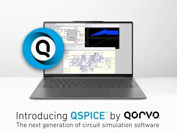
Qorvo® QSPICE™ Revolutionizes Circuit Simulation for Power and Analog Designers

GREENSBORO, NC, Oct. 25, 2023 /PRNewswire/ — Qorvo® (Nasdaq: QRVO), a leading global provider of connectivity and power solutions, recently announced the release of QSPICE™, a new generation of circuit simulation software that provides power and analog designers significantly higher levels of design productivity through improved simulation speed, functionality and reliability.

In addition to advancing the state of the art in analog simulation technology, QSPICE allows designers to simulate complex digital circuits and algorithms. Its unique combination of modern schematic capture and fast mixed-mode simulation make it the ideal tool to solve the increasingly complex hardware and software challenges faced by today’s system designers.


“QSPICE enables an entirely new generation of mixed-mode circuit simulation,” said Jeff Strang, general manager for Qorvo’s Power Management business. “In the past, power designers relied on analog circuits and silicon power switches. Today, digital control and compound semiconductors are common elements of advanced power designs. Whether an engineer is developing AI algorithms for EV battery charging, optimizing a Qorvo pulsed-radar power supply or evaluating the newest silicon carbide FETs, QSPICE is the perfect platform for innovation.”

Qorvo’s QSPICE is available free of charge and offers numerous enhancements over legacy analog modeling tools. These improvements include:

  • Complete support for advanced analog and digital system simulations, such as those used in AI and machine-learning applications.
  • An upgraded simulation engine that uses advanced numerical methods and is optimized for modern computing hardware, including a GPU-rendered user interface and SSD-aware memory management, to provide dramatically higher speed and accuracy.
  • Reduced overall runtimes and a 100% completion rate, based on Qorvo benchmark tests with a suite of challenging test circuits. This compares to a failure rate of up to 15% with these same test circuits using other popular SPICE simulators.
  • Availability of a regularly updated QSPICE model library featuring Qorvo’s silicon carbide and advanced power management solutions, making it easy for customers to evaluate and design with Qorvo power.

QSPICE is available now at www.qspice.com and is actively supported by Qorvo as well as a robust user community through Qorvo’s QSPICE forum at forum.qorvo.com.

About Qorvo
Qorvo (Nasdaq: QRVO) supplies innovative semiconductor solutions that make a better world possible. We combine product and technology leadership, systems-level expertise and global manufacturing scale to quickly solve our customers’ most complex technical challenges. Qorvo serves diverse high-growth segments of large global markets, including consumer electronics, smart home/IoT, automotive, EVs, battery-powered appliances, network infrastructure, healthcare and aerospace/defense. Visit www.qorvo.com to learn how our diverse and innovative team is helping connect, protect and power our planet.

Click here to read Qorvo’s forward-looking statementshttps://www.qorvo.com/newsroom/news/2023/qorvo-qspice-revolutionizes-circuit-simulation-for-power-and-analog-designers

Supermicro highlights AI as next industrial revolution; foundation of new era lies with digital data creation, storage, and processing

TAIPEI, Oct. 12, 2023 /PRNewswire/ — In 2024, the semiconductor sector will face several major changes. At the forefront of these changes are innovations in high-performance computing (HPC) and AI server supply chains. DIGITIMES will spotlight these transformations at the “2024 Next-Gen Intelligence Symposium” on November 3, 2023. The event will feature insights from DIGITIMES’ senior analysts and industry experts from Supermicro, with the aim to offer a deep understanding of Asia’s supply chain dynamics and the evolving tech landscape.

Credit: DIGITIMES
Credit: DIGITIMES

Alok Kumar Srivastav, a senior solutions manager at Supermicro, will speak at the event. He’s mainly responsible for businesses related to AI, machine learning, and HPC. He will discuss how AI is at the tipping point of transforming industries in his keynote titled “Ushering in a New Era of AI with Modern Building Blocks.”

In a recent interview with DIGITIMES Asia, Srivastav discussed the fundamental modern building blocks that are enabling AI, what industries are already adopting AI, balancing between key partners like Nvidia, Intel, and AMD, and how AI will affect the server/infrastructure industry and beyond in the future.

The digital era is the cornerstone of the AI

Srivastav pointed out during the interview that the key technologies pushing AI into a new era are digitalization, storage, and accelerated computing, and Supermicro’s solutions cover all of its customers.

All of these are related to the one true foundation of AI: digital data. The one requirement for AI to work is a well-trained model, and a well-trained model needs a lot of digital data.

The digitalization helps fulfill the first step of this process. The recent digital explosion meant that we were creating a lot more data. In fact, according to Srivastav, over 90% of existing data in the world was generated in the last 2-3 years.

Once the digital data is created, Storage technology is mature enough to handle this massive amount of new data accordingly at different stages of its life cycle.

The final and most crucial is accelerated computing capability. Advancements in modern computing capabilities have enabled corporations to process and convert complex digital data into meaningful insights.

A cross-industry phenomenon

As with the industries that are looking to or have already adopted AI, Srivastav listed a long list of industries that are already under Supermicro’s umbrella. These industries include automotive (esp. EVs), cloud computing (that caters to specific types of workloads), energy (oil/gas), financial, healthcare, higher education, media and entertainment, the public sector, HPCs, telecommunications, and more.

While Srivastav declined to name a specific company, he ensured that these are all major corporations that are leaders in their respective industries. When it comes to volume, he mentioned that because of the demand for new infrastructure due to the emergence of cloud computing, almost all these major corporations are procuring “thousands of computing units from Supermicro.”

Achieving a balance between key partners

One of the more interesting parts of Supermicro’s business is that it’s agnostic and works very closely with key partners like Intel, Nvidia, and AMD, companies that are actively competing against each other in the same sector. When asked about this, Srivastav admitted that keeping pace with the innovation and progress of all three companies is not an easy task.

“Supermicro’s DNA is first-to-market, and we want to be first for all of our state-of-the-art products and all of our customers,” he stated.

‘The Fourth Industrial Revolution’

Regarding the future direction of the industry, Srivastav pointed out that advancements in AI technology have resulted in lower error rates and have allowed more and more corporations to become more accepting of this technology.

All of this will lead to something they referred to as “the fourth industrial revolution.” This revolution will be powered by two main technologies: AI and IoT. The change and impact of this revolution will be so profound that it will affect all industries in the world, be it design or manufacturing. It’ll no longer be “if” you want to adopt AI but rather “when and how soon” to adopt AI to survive in the modern marketplace.

Srivastav stated that AI will become like electricity; so widely adopted and accepted that you won’t even question its existence. You will come to accept it as part of your day-to-day life. In fact, there are already many instances of AI use in our daily lives (such as autocomplete) that we just don’t realize. We are already consumers of AI.

If you would like to attend the 2024 Next-Gen Intelligence symposium in person on Nov 3, 2023, Please Register now!

Alok Kumar Srivastav, senior solutions manager at Supermicro. Credit: Supermicro

Media contact: joyce.siow@digitimes.com