Tag Archives: SEM

RS Components is stocking an extensive range of RS PRO handheld T&M instruments

RS own brand range includes digital multimeters, voltage/current calibrators, insulation testers, temperature calibrators, and voltage indicators

JAKARTA, Indonesia, Dec. 28, 2020RS Components (RS), a trading brand of Electrocomponents plc, a global omni-channel solutions partner for industrial customers and suppliers, is now stocking in Indonesia an extensive range of RS PRO handheld test and measurement instruments for engineers and technicians on the go. The range includes devices that allow accurate and ergonomic measurements and calibration, including handheld multimeters, clamp meters and voltage indicators, and all the necessary accessories.

The RS PRO handheld T&M instrument range also includes the RS PRO insulation tester to help technicians ensure the wiring insulation is safe and remains undamaged after electrical work has been completed.

The RS PRO RS14 digital multimeter is a useful instrument for measuring capacitance, voltage, electrical current, and resistance and features a diode and continuity check.

All RS PRO products and equipment have been through high-calibre compliance and quality testing to assure quality, durability, and consistency, and come with the RS PRO Seal of Approval.

The RS PRO handheld T&M equipment range is shipping now from RS in Indonesia.

About RS Components

RS Components is a trading brand of Electrocomponents plc, a global omni-channel solutions partner for industrial customers and suppliers who are involved in designing, building or maintaining industrial equipment and facilities. We aim to offer our customers unrivalled choice of product technologies, solve problems with innovative solutions and deliver a world-class customer experience, making it easy to do business with us.

We stock more than 500,000 industrial and electronic products, sourced from over 2,500 leading suppliers. We solve problems and provide a wide range of value-added solutions to over one million customers. With operations in 32 countries, we trade through multiple channels and ship over 50,000 parcels a day.

Electrocomponents plc is listed on the London Stock Exchange and in the last financial year ended 31 March 2020 reported revenue of £1.95 billion. Electrocomponents plc has six operating brands; RS Components, Allied Electronics & Automation, RS PRO, OKdo, DesignSpark and IESA.

For more information on RS, please visit the website at https://www.rs-online.id/.

Further information is available via these links:
Twitter: @RSComponents; @designsparkRS
Linkedin: www.linkedin.com/company/rs-components

RS Components
https://www.rs-online.id/
DesignSpark
www.rs-online.com/designspark
Electrocomponents plc
www.electrocomponents.com

Contact:

Virginie Cosentino
virginie@budcomms.com
+65-9161-5091

Related Links :

https://www.rs-online.id/

RS Components announces availability of Phoenix Contact ‘COMPLETE line’ range for control cabinet applications

KANAGAWA, Japan, Dec. 21, 2020  — RS Components (RS), a trading brand of Electrocomponents plc (LSE: ECM), a global omni-channel solutions partner for industrial customers and suppliers, today announced the significant expansion in Japan of its ‘COMPLETE line’ portfolio of products and essential accessories for control cabinet applications from Phoenix Contact, one of the world’s leading makers of industrial automation technologies.

This expansion of more than 2500 new devices means that RS is the first high-service distributor to offer the full ‘COMPLETE line’. This means customers will gain full access to a unique portfolio that will help to reduce handling costs and minimise planning and installation times for control cabinet construction and maintenance.

The ‘COMPLETE line’ system comprises an entire suite of coordinated hardware and software products that help panel builders to optimise their work processes in control cabinet development. The system brings together all of the manufacturer’s control panel products and essential accessories in one range, making it significantly easier to purchase, install and operate existing and new control cabinet solutions.

Phoenix Contact COMPLETE line

Due to the range’s standardised design, haptics and functionality, along with standardised marking, bridging and testing accessories, the system also results in simple and intuitive handling of all the hardware, saving engineers significant installation, start-up and maintenance time. More than 3000 devices in the ‘COMPLETE line’ range use the same push-in connection technology, helping to reduce connection time by up to 70%. In addition, the manufacturer’s planning and marking ‘PROJECT’ software has an intuitive user interface that makes it easy in the planning, automatic checking and ordering of terminal strips.

Aimed at switching, connection and disconnection, as well as measuring, controlling and automation applications, the extensive portfolio comprises thousands of devices including DIN rails and terminals, PLCs and HMIs and heavy-duty connectors. Highlights include the latest PTFIX distribution blocks with push-in connection, machine safety devices including the latest release PSR series of safety relays and I/O and PLC expansion modules, which is part of the PLCnext ecosystem from Phoenix Contact.

Comprising more than 9000 products, RS is increasing its Phoenix Contact portfolio in all the key areas of building control cabinets. All of the devices in the ‘COMPLETE line’ portfolio are shipping now from RS in Japan and across Asia Pacific.

Related Links :

https://jp.rs-online.com

QuantalRF secures CHF17M / $19M Series B funding to develop and commercialize disruptive RF front-end solutions


ZÜRICH and SAN DIEGO, Dec. 16, 2020QuantalRF, an emerging RF semiconductor company developing transformative wireless communication solutions, has announced the closing of an oversubscribed Series B funding round, resulting in CHF17 million / $19 million. The growth equity round was led by Zürich based Metellus AG and Dara Capital Ltd., alongside existing shareholders and family offices.

The new funding will be used primarily to accelerate the commercialization of QuantalRF’s patented RF front end technologies, expand the engineering team, and to rapidly scale the product development of 5G/UHB (Ultra High Band) and Wi-Fi 6/6e front-end IC components.

The funding round builds on an exceptional year for QuantalRF which saw the addition of a new CEO/CTO, a successful evaluation of its Quantal Amplifier Technology and received samples for their first Quantal RFIC.

"I am very excited about the direction of QuantalRF and how we are continuing to shape our Quantal Technology to address the challenges the RF front-end market is facing," said Dr. Ali Fard, QuantalRF CEO/CTO. "Throughout this year we have received valuable insights and positive feedback on our technology through extensive third-party evaluations provided by our partners and customers. The focus for our next development phase is to address the demand for integrated RF filters used in wireless standards that require wide bandwidth while maintaining good wideband performance and very sharp cut-off filtering."

"Our investors not only see the enormous opportunity in the development of next generation RF front-end, more importantly, they see the advantage and unique position QuantalRF has to be a disruptive force in driving this market. The support and confidence shown from our investors is validation of our mission and of the team we have assembled," said Antonio J. Viana, Executive Chairman. "The Board of Directors, along with our investment community, are extremely excited to see QuantalRF move into its next phase of growth and development."

About QuantalRF

QuantalRF is an emerging RF semiconductor company developing transformative wireless communication solutions to redefine the user experience. As an innovator of high-performance RF semiconductors, focused on front-end IC parts such as Power Amplifiers (PA), Low Noise Amplifiers (LNA), on-chip Filters focused on a wide range of communication systems including Wi-Fi 6/6e and 5G UHB (Ultra-High Band), QuantalRF is creating novel solutions to address to emerging connectivity needs of RF wireless systems.

At QuantalRF we are transforming the RF front-end with ultra-compact solutions rivalling acoustic wave and GaAs performance in highly integrated CMOS-SOI technology for commercial applications, including millimeter wave. We leverage our patented Quantal Technology in disruptive RF front-end solutions that significantly improve area, cost, power consumption and overall performance.

QuantalRF was established based on the inventions of Co-Founder and former NASA scientist, Dr. Forrest J. Brown.  These inventions developed into our RF front-end technology known as Quantal Technology. Headquartered in Zürich, Switzerland, with operations in the USA and Sweden, QuantalRF has an impressive portfolio of over 250 granted patents and applications with broad geographic coverage.

For more information, please visit www.quantalrf.com 

Logo – https://techent.tv/wp-content/uploads/2020/12/quantalrf-secures-chf17m-19m-series-b-funding-to-develop-and-commercialize-disruptive-rf-front-end-solutions.jpg

Related Links :

Home

YES Partners with Singapore’s Gaia Science

Specialists in SEA, China science & biotech equipment market to expand YES’s global reach

FREMONT, Calif., Dec. 7, 2020 — YES (Yield Engineering Systems, Inc.), a leading manufacturer of process equipment for semiconductor advanced packaging, Life Science and "More-than-Moore" applications, today announced that it has signed an agreement with Gaia Science Pte. Ltd of Singapore to sell and service YES equipment in southeast Asia and mainland China. 

The partnership, which began in early September, is expected to be particularly helpful in showcasing YES’s monolayer coating and plasma cleaning products to the region’s dynamic Life Science Industries.

"We see considerable synergy between our products and Gaia’s expertise in the areas of microfluidics, engineering polymers, genomics, 3D printing, DNA diagnostics, and oligonucleotides research. That synergy, together with both our companies’ experience in semiconductors, gives us high hopes for this new venture," said Rezwan Lateef, President of YES.

"YES products are well-accepted among the world’s leading Life Science companies, and we look forward to strengthening our relationships with these customers in our region. We see a very good fit for YES products in our portfolio. With our extensive coverage of the Life Science and physical science markets, we expect to leverage the capabilities that YES products bring to both the biotech and semiconductor sectors," said Ms Weng Lijuan, Managing Director at Gaia.

About YES

YES (Yield Engineering Systems, Inc.) is a leading manufacturer of high-tech, cost-effective equipment for transforming surfaces, materials and interfaces.  The company’s product lines include vacuum cure ovens, chemical vapor deposition (CVD) systems, and plasma etching tools used for precise surface modification and thin-film coating of semiconductor wafers, semiconductor and MEMS devices, biosensors and medical substrates. With YES, customers ranging from startups to Fortune 100 companies can create and volume-produce products in a wide range of markets, including Advanced Packaging, MEMS, Augmented Reality/Virtual Reality and Life Sciences. YES is headquartered in Fremont, California, with a growing presence globally. For more information, please visit www.yieldengineering.com.

Media Contact

Victoria Barnes
Director of Communications
YES (Yield Engineering Systems, Inc.)
510-954-6723 direct
VBarnes@yieldengineering.com

About Gaia

Based in Singapore, Gaia Science Pte. Ltd has extensive experience supplying state-of-the-art scientific and laboratory equipment to universities, research institutions and industries. The company is recognized for bringing cutting-edge technologies from its partners and principals to customers working in application areas such as genomics, proteomics, cell biology, animal research, organic synthesis, nanotechnology, clean energy research, environmental analysis, imaging, and education. Besides providing turnkey laboratory solutions to its customers, Gaia Science is also involved with international partners in the design and manufacturing of bioengineering products. For more information, please visit www.gaiascience.com.sg.

Related Links :

home

InnoLight Announced Availability of Industry’s First 800G Pluggable OSFP and QSFP-DD800 Transceivers at ECOC 2020

SUZHOU, China and SANTA CLARA, Calif., Dec. 4, 2020 — InnoLight Technology (Suzhou) Ltd., the leader in data center optics, will demonstrate video demos of 800G pluggable OSFP 2xFR4, 800G OSFP DR8+ and QSFP-DD800 DR8+ at ECOC 2020 online event. See these products and video demos at InnoLight virtual Booth #673.

New applications such as work-from-home cloud collaboration, self-driving cars, remote medicine, and artificial intelligence have brought a surge in data traffic. Global data volumes are expected to double every 2-3 years into the next decade. How to balance the demand for bandwidth, cost, and power consumption, and to achieve smooth network transition is a continuing challenge facing the industry. To support this rapid growth and network transition, InnoLight is introducing a line of 800G OSFP and QSFP-DD800 optics. OSFP 2xFR4 and DR8+ are currently available for early customer evaluation, with QSFP-DD800 DR8+ available in January 2021. Other 800G parts as listed below will be ready for evaluation in 1H 2021. Volume production is currently planned for either Q4, 2021 or Q1 2022 depending upon product type. 

  • 800G OSFP 8x100G DR8 & AOC
  • 800G OSFP DR8+
  • 800G OSFP 2x400G FR4
  • 800G OSFP 1x800G LR8
  • QSFP-DD800 8x100G DR8 & AOC
  • QSFP-DD800 DR8+
  • QSFP-DD800 2x400G FR4
  • QSFP-DD800 8x100G LR

In addition to the above mentioned 800G products, InnoLight is developing innovative optics to enable 800G transmission in the legacy 4X fiber structure in either multimode OM3/OM4 or single mode fiber plant. These innovative optics will help customers to increase bandwidth to 800G using the existing SR4 or DR4 fiber layouts for point to point or breakout applications. Availability is planned in 2H 2021.

"InnoLight’s 800G transceivers continue InnoLight’s leadership in high performance pluggable optics, doubling bandwidth capacity without disruption of existing data center infrastructure. With our industry leading 400G deployments, InnoLight is uniquely positioned in driving 800G implementation and to deliver the best price performance optics in the industry. Our new innovative 800G optics to support existing 4x fiber plants are especially suited for Hyperscale DC operators." said Osa Mok, Chief Marketing Officer of InnoLight.

During ECOC, InnoLight will also demonstrate its 100G/200G/400G coherent solutions. These new generation coherent pluggable modules can support DCI, Metro, and 5G backhaul transport networks.

  • 400G OSFP ZR & OpenZR+
  • 400G QSFP-DD ZR & OpenZR+
  • 400G CFP2 OpenZR+ / Metro
  • 100G QSFP-DD OpenZR+

About InnoLight

InnoLight designs, builds and markets high-speed optical transceivers that enable rapid bandwidth expansion of next generation networks. It is headquartered in Suzhou, China with manufacturing locations in China, Taiwan and Thailand. It has RD and Sales offices in China, US, and Singapore.  InnoLight’s solutions offer superior technical performance, compelling value proposition, and time to market advantages that are critical for the sustaining growth of the Data Center, 5G Wireless and Metro Network. For additional information, please visit www.innolight.com.

Related Links :

http://www.innolight.com

China moves closer to self-reliance in 7nm chip production

BEIJING, Nov. 27, 2020 — A news report by China.org.cn on China moves closer to self-reliance in 7nm chip production.

China has recently made new breakthroughs in its 7nm chip-making process, reportedly developing tools and know-how for several segments of the manufacturing process amid efforts to reduce reliance on foreign equipment and material vendors.

Last month, China’s chip customization solution provider Innosilicon announced that it had taped out and completed testing of a prototype chip based on the FinFET N+1 process of Semiconductor Manufacturing International Corporation (SMIC). This achievement marks a new step forward in China’s homegrown chip development.

An exhibition booth of China's Semiconductor Manufacturing International Corporation (SMIC) is seen at the 17th China International Semiconductor Expo in Shanghai, Sept. 3, 2019. [Photo/CFP]
An exhibition booth of China’s Semiconductor Manufacturing International Corporation (SMIC) is seen at the 17th China International Semiconductor Expo in Shanghai, Sept. 3, 2019. [Photo/CFP]

Amid major trade restrictions enforced by the United States, SMIC’s new generation foundry node is said to be comparable to the 7nm process by Taiwan Semiconductor Manufacturing Company (TSMC), the world’s largest dedicated independent semiconductor foundry.

As China’s largest chip foundry, SMIC will introduce its N+1 7nm node, marking a significant improvement over its current 14 nm production node, boasting a 20% increase in performance, power consumption reduction of 57%, a reduced logic area of 63%, and SoC (System on a Chip) area reduction of 55%, according to the company.

Moreover, the N+1 foundry node may enable SMIC to break its reliance on advanced Extreme Ultraviolet (EUV) lithography machines produced by Dutch microchip machine maker ASML, according to Liang Mengsong, co-CEO of SMIC. ASML is subject to U.S. export controls as its products contain American technology.

At the same time, China is working hard to develop its own lithography system.

The Suzhou Institute of Nano-tech and Nano-Bionics under the Chinese Academy of Sciences (Sinano), along with the National Center for Nanoscience and Technology, recently announced a breakthrough in a new type of 5nm laser lithography technology. Experts believe it could lay the foundation for research into a self-developed advanced lithography machine.

The new technology has broken the traditional constraint in laser direct writing (LDW) with its ability to process at the nano level. In addition to ultra-high precision, the technology also demonstrates potential for mass production.

According to research results published in Nano Letters, a monthly peer-reviewed scientific journal, the new LDW technology "exhibits an attractive capability of well-site control and mass production of 500,000 nanogap electrodes per hour," breaking the trade-off between resolution and throughput using nanofabrication techniques.

During the recent China International Import Expo (CIIE) in Shanghai, ASML, the global leader in lithography machines, showcased its deep ultraviolet (DUV) lithography machines, sending out a strong signal for its capability and willingness to export the equipment to China.

Previously, ASML’s CFO Roger Dassen has stated that the company can export DUV lithography machines to China without a U.S. license. The technology can typically produce chips down to the 7nm node.

On the side of materials, Nata Opto-electronic Materials in east China’s Jiangsu province announced that it has established China’s first ArF photoresist production line, which is used to transfer electronic circuit patterns to silicon crystals in the 7nm chip-making process.

Previously, photoresist materials produced in China could only be applied in the production of chips with standards of 436nm and 365nm.

As the world’s largest semiconductor market, China has been spending aggressively in semiconductor investment, acquisition, and talent recruitment to bolster the industry by on-shoring chip manufacturing equal to those of the world’s top foundries.

A report by Goldman Sachs on July 2 predicted that China may be capable of producing 7nm chips by 2023.

Thomas Friedman, a columnist for the New York Times, said during an online forum on Nov. 11 that China attempts to build an entire microchip supply chain from end to end, and will be no longer dependent on the U.S. technologies, according to the country’s latest five-year plan.

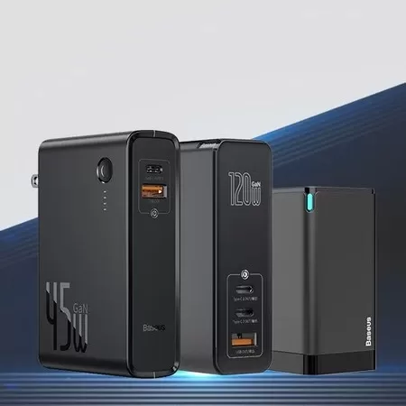
Baseus Announces New Gallium Nitride (GaN) Series 120W Charging Heads

AUGSBURG, Germany and HILLIARD, Ohio, Nov. 26, 2020 — By virtue of the advanced research and development technology and excellent quality, Baseus, the well-known brand in domestic consumer electronics industry, has brought a variety of high-quality products to consumers. Baseus grandly launched 45W/65W/120W new Gallium Nitride (GaN) Series 120W Charging Heads leading the entire charging industry.

Baseus GaN series Quick Chargers

First of all, the company has to introduce the First 65W Triple-port Quick Charging plug on the market, which can be used for charging three devices at the same time. This charger is not only compatible with mainstream charging protocols such as QC and PD, but also supports SCP and FCP. It can fast charge laptops, phones, NS, smart wearable devices, etc. There’s nothing to worry about charging even if consumers need to carry multiple digital devices on a trip.

The second is 120W Charging Plug. This product is mainly designed for charging laptops, up to 100W 20V/5A. It can fast charge two laptops simultaneously, compatible with MacBook, Dell, HP, Lenovo and more.

Another one is 45W 2-in-1 Charging Plug, which supports quick charging, and can be used as a 10000mAh power bank. The Type-C port supports charging up to 30W 20V/2.25A.

As people all know, GaN chargers are smaller and more powerful than traditional chargers, making them ideal for using at home, in the office or for business trip.

Compared with other products on the market that are made of GaN only, Baseus three new products are able to achieve Higher Frequency, Smaller Size, Higher Efficiency and Lower Temperature Rise via adopting the Third-generation Semiconductor Materials, GaN and SiC.

Baseus GaN series adopts industrial-grade LLC resonant circuit and half-bridge architecture with two GaN MOS switches. The LLC architecture contains a resonant inductor and resonant capacitor, and two transformers are a output main transformer and resonant circuit-drive transformer. Therefore it realizes higher efficiency with high-power power supply. The half-bridge architecture with two GaN MOS switches requires less on voltage withstand value of devices, to achieve greater output power and higher output efficiency.

A variety of models of 65W, 120W, 45W 2-in-1 chargers offered by Baseus are advanced products leading the industry in terms of configuration. Also the powerful product lines are unparelled by other brands. They also offer different ports and colors, which maximally meets the diverse needs of consumers and is favoured by white collar workers, businessmen and technology enthusiasts. Till October 2020, Sales Volume of Baseus GaN Series Products has reached One Million pcs.

"Charge Fast, Baseus First" Baseus has been taking the fastest action to bring faster and safer charging experience to consumers all around the world.

Baseus is derived from the brand’s slogan Base on User, which represents their insistence on thinking from the user’s point of view. As a core, everything they do is based on the users, creating simple and practical products to constantly enrich the user’s life.

Baseus insists on designing innovation, focusing on technical and quality strength. Centered by Baseus, they developed and produced Baseus Games, Music, Lighting, Car Products and Home Appliances to meet users’ needs for more intelligent products.

Related Links:
https://amzn.to/38TrkuM

Press Contacts:
Address: 4340 Lyman Dr., Hilliard, OH 43026, United States
Albert Ou – Public Relations Specialist
Email:  vipbaseus@gmail.com
Phone: +86 13530560435


Related Links :

http://www.baseus.com

Semicon Light, a company possessing the original technology of silver free-flip chip LED, will actively respond to patents

YOUNGIN-SI, South Korea, Nov. 12, 2020 — Semicon Light plans to actively respond to the patents to protect the original technology, "Silver- Free Flip Chip LED".

Logo of SEMICON LIGHT Co., Ltd

Semicon Light, a company specializing in manufacturing flip-chip LEDs, developed the silver-free flip-chip technology for the first time and holds original patents related to the flip-chip LEDs’ reflective layer. It is a Korean LED chip manufacturer listed on the KOSDAQ market in 2015, and has about 250 flip chip LED-related patents registered in Korea and other countries such as the United States and China.

Semicon Light’s silver-free flip chip is a new type of flip chip instead of the existing horizontal LED chip, and adopts a method of inverting the LED chip and directly fusing it onto the substrate without separate wire bonding. It is a technology that can realize ultra-high reflectance and high reliability through the oxide matirials(DBR, Distributed Bragg Reflector). In addition, it can significantly improve the performance of the elements by being easily applied to ultra-small LEDs such as Mini or Micro LEDs, which are rapidly forming the market recently.

The industry predicts that the display market based on mini LEDs will be formed in earnest from next year prior to realizing the display using micro LED, which is the final and ultimate display technology. In fact, according to a report by the market research firm, Trend Force, it is predicted that mini LED TVs will compete equally with W-OLED (White Organic Light-Emitting Diode) TVs in the premium TV market next year.

With such changes in the display markets, flip-chip LED has become an essential technology, not an option. It is expected that Semicon Light’s ‘Silver Free Flip Chip’ technology, which can make LED chips small while maintaining high performance and high reliability, will emerge as an important element technology. It is found that several large LED chip manufacturers in Taiwan and mainland China are adopting the related technologies.

In this context, Semicon Light intends to materialize the patent strategies and will make every effort to secure the competitiveness of our own technologies by actively responding to patent infringement.

According to company officials, "Semicon Light has world-class LED technologies. In particular, we plan to proactively assert our rights against indiscriminate infringement of intellectual property by establishing a dedicated organization to protect our original technologies.

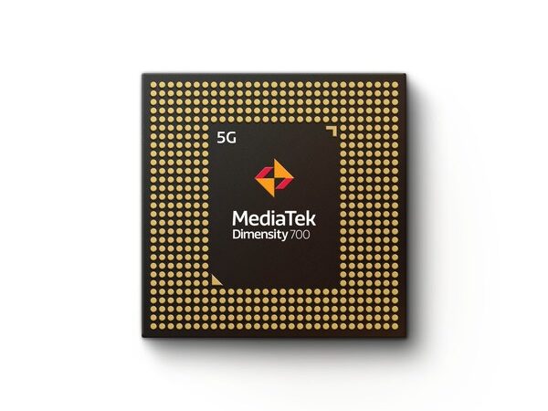
MediaTek Unveils Its Newest 5G Chipset, Dimensity 700, For Mass Market 5G Smartphones

Dimensity 700 caters to growing consumer demand for 5G devices

HSINCHU, Taiwan, Nov. 11, 2020 — MediaTek today unveiled its new Dimensity 700 5G smartphone chipset, a 7nm SoC designed to bring advanced 5G capabilities and experiences to the mass market. The addition of the Dimensity 700 to MediaTek’s Dimensity family of 5G chips gives device makers a full suite of options for 5G smartphone models – from flagship and premium to mid-range and mass market devices – making 5G more accessible for consumers everywhere.

Dimensity 700
Dimensity 700

"With our expanded Dimensity portfolio we’re bringing the latest 5G capabilities to every smartphone tier so more people can enjoy 5G experiences," said Dr. JC Hsu, Corporate VP and GM of MediaTek’s Wireless Communications Business Unit. "The Dimensity 700 has an impressive mix of 5G connectivity features, advanced camera capabilities like night shot enhancements and multiple voice assistant support, all in a super power-efficient design."

The Dimensity 700 packs advanced connectivity features including 5G Carrier Aggregation (2CC 5G-CA) and 5G dual SIM dual standby (DSDS), giving users access to the fastest speeds and 5G-exclusive Voice over New Radio (VoNR) services from either connection. On the processing power side, the chip integrates two Arm Cortex-A76 big cores in its octa-core CPU and operates at up to 2.2GHz.

Key features of Dimensity 700 include:

  • MediaTek 5G UltraSave: Delivers advanced power-saving technologies to improve battery life. It includes UltraSave Network Environment Detection, MediaTek 5G UltraSave OTA Content Awareness, Dynamic BWP and Connected Mode DRX. The built-in technology intelligently manages a device’s 5G connection so you can do more and charge your device less often.
  • Premium 90Hz Display: Brands can design smartphones with crisp, high resolution FullHD+ displays and ultra-fast refresh rates to reduce blur in animations, scrolling and games for the best user experience.
  • Up to 64MP Cameras & Night Shot Enhancements: Supports 48MP or 64MP main camera sensors with AI-bokeh, AI-color and AI-beauty features. Plus, the integrated hardware-based imaging accelerators enable multi-frame noise reduction so users can capture high quality shots with low noise, even at night.  
  • Multiple Voice Assistant Support: Supports voice assistants from global brands such as Alibaba, Amazon, Baidu, Google and Tencent to give device makers more configuration options.

Dimensity 700 Infographic

The Dimensity 700 continues MediaTek’s legacy of bringing advanced connectivity, multimedia and imaging features to consumers everywhere. MediaTek’s Dimensity 5G family of chips bring smart and fast together to power 5G devices across all tiers, and with the Dimensity 700 5G devices will now be accessible to even more consumers.

For full specifications and further details on MediaTek’s Dimensity 700 series and 5G portfolio visit: https://i.mediatek.com/mediatek-5g

About MediaTek Inc.

MediaTek Incorporated (TWSE: 2454) is a global fabless semiconductor company that enables 1.5 billion connected devices a year. We are a market leader in developing innovative systems-on-chip (SoC) for mobile device, home entertainment, connectivity and IoT products. Our dedication to innovation has positioned us as a driving market force in several key technology areas, including highly power-efficient mobile technologies, automotive solutions and a broad range of advanced multimedia products such as smartphones, tablets, digital televisions, 5G, Voice Assistant Devices (VAD) and wearables. MediaTek empowers and inspires people to expand their horizons and achieve their goals through smart technology, more easily and efficiently than ever before. We work with the brands you love to make great technology accessible to everyone, and it drives everything we do. Visit www.mediatek.com for more information.

MediaTek Press Office:

PR@mediatek.com
Kevin Keating, MediaTek
+1- 206-321-7295
10188 Telesis Ct #500, San Diego, CA 92121, USA

Related Links :

http://www.mediatek.com

USI Strives Toward Industry 4.0 through the Deployment of Smart Manufacturing

SHANGHAI, Nov. 10, 2020 — The development of smart manufacturing and industry 4.0 concepts in the manufacturing industry has become a key strategy for companies seeking to improve quality, safety and advance their technology. USI (SSE: 601231), a leading electronics designer and manufacturer in the world, is improving productivity standards and manufacturing quality through the deployment of networked infrastructure, automatic data collection, real-time monitoring and analysis, big data analysis, electronic reports and parameter management. 

Auto Material Handling System (From Warehouse to Shop Floor)

In recent years, the manufacturing industry has undergone profound changes. A low-cost business model is no longer competitive enough to meet the rising demands of a transformed industry that has moved up the value chain, nor resist the advent of smart manufacturing. "USI is adopting smart manufacturing to enhance our competitiveness through the digitalization of our production processes including the automation of infrastructure and logistics using robotics and automated guided vehicles," said Jim Cao, General Manager of Greater Shanghai and Smart Manufacturing/SiM BU, USI. "In addition, we are establishing real-time management and control, online quality and parameter management systems, that will assist our engineers in preempting, troubleshooting and analyzing data, in order to achieve a smart manufacturing environment," he continued.

With the increasing complexity of SiP (System-in-Package) technologies and the need to maintain a competitive lead, USI established a flagship smart manufacturing factory at its Zhangjiang, Shanghai facility in 2013. USI’s smart manufacturing division and the R&D Engineering team have co-developed an integrated production facility test and inspection system that enables efficiency and quality in the production process. The implementation of equipment automation has already demonstrated significant positive impacts, and the number of automation programs introduced by USI will continue to increase at a rate of 20% each year.

USI adopts the IIoT (Industrial Internet of Things) concept to establish a smart manufacturing ‘5-star rating’ system (for example; 100% automation, over 80% of production lines adopting lights off manufacturing, less than 30% direct manpower) that combines big data and industry standards. USI has 9 factories in the world, among which is the Zhangjiang Factory in Shanghai that boasts the highest level of automation. USI is planning to transform all its factories into 3-star and 4-star levels by 2023 and upgrade four of its factories into lights out factories (5-star level) by 2025. By that time, all the machinery in the lights out factories will be connected to the internet, and a parameter management system will be established. Achieving complete automation in manufacturing will reduce human error and raise product quality, whilst an automated logistics system will help connect remote sites to enable real-time production monitoring and increase production efficiency.

About USI

USI (SSE: 601231, A constituent of CSI300 Index), Universal Scientific Industrial (Shanghai) Co., Ltd., is a global leader in electronic design and manufacturing as well as a leader in the field of SiP (System in Package) modules. USI provides D (MS)2 product services: Design, Manufacturing, Miniaturization, Industrial software and hardware Solutions, and material procurement, logistics and maintenance Services. With a sales and service network in America, Europe, and Asia; and manufacturing sites in Mainland China, Taiwan, Mexico and Poland, USI offers customer diversified products in the sectors of wireless communication, computer and storage, consumer, industrial, and automotive electronics worldwide. USI is one of subsidiaries of ASE Technology Holding Co., Ltd. which is the leading provider of semiconductor manufacturing services in assembly and test in the world. To learn more, visit www.usiglobal.com and engage with us on LinkedIn and YouTube.