Tag Archives: NAN

EV Group Brings Revolutionary Layer Transfer Technology to High-Volume Manufacturing with EVG®850 NanoCleave™ System


Infrared laser cleave technology enables ultra-thin-layer transfer from silicon substrates with nanometer precision, revolutionizing 3D integration for advanced packaging and transistor scaling

ST. FLORIAN, Austria, Dec. 8, 2023 /PRNewswire/ — EV Group (EVG), a leading supplier of wafer bonding and lithography equipment for the MEMS, nanotechnology and semiconductor markets, today introduced the EVG®850 NanoCleave™ layer release system—the first product platform to feature EVG’s revolutionary NanoCleave technology. The EVG850 NanoCleave system enables nanometer-precision release of bonded, deposited or grown layers from silicon carrier substrates using an infrared (IR) laser coupled with specially formulated inorganic release materials in a proven, high-volume-manufacturing (HVM) capable platform. As a result, the EVG850 NanoCleave eliminates the need for glass carriers—enabling ultra-thin chiplet stacking for advanced packaging, as well as ultra-thin 3D layer stacking for front-end processing, including advanced logic, memory and power device formation, to support future 3D integration roadmaps. 

View inside the EVG®850 NanoCleave™ layer release system, with the pre-processing module bay and the mechanical release module in the background. Source: EV Group.

The first EVG850 NanoCleave systems have already been installed at customer facilities, and nearly two dozen product demonstrations are underway with customers and partners at customer sites and EVG’s headquarters.

Silicon Carriers Benefit 3D Stacking and Back-end Processing 
In 3D integration, glass substrates have become an established method for building up device layers through temporary bonding with organic adhesives, using an ultraviolet (UV) wavelength laser to dissolve the adhesives and release the device layers, which are subsequently permanently bonded onto the final product wafer. However, glass substrates are difficult to process with semiconductor fab equipment that have been designed primarily around silicon, and that require costly upgrades to enable glass substrate processing. In addition, organic adhesives are generally limited to processing temperatures below 300 °C,  limiting their use to back-end processing.

Enabling silicon carriers with inorganic release layers avoids these temperature and glass carrier compatibility issues. In addition, the nanometer precision of IR laser-initiated cleaving allows for processing extremely thin device wafers without changing processes of record. Subsequent stacking of such thin device layers enables higher-bandwidth interconnects and new opportunities to design and segment dies for next-generation, high-performance devices.

Next-generation Transistor Nodes Require Thin-layer Transfer Processes
At the same time, transistor roadmaps for the sub-3-nm node call for new architectures and design innovations such as buried power rails, backside power delivery networks, complementary field-effect transistors (CFETs) and 2D atomic channels, all of which require layer transfer of extremely thin materials. Silicon carriers and inorganic release layers support process cleanliness, material compatibility and high processing temperature requirements for front-end manufacturing flows. However, until now, silicon carriers had to be completely removed using grinding, polishing and etching processes, which results in micron-range variations across the surface of the working device layer, making this method unsuitable for thin-layer stacking at advanced nodes.

“Releasable” Fusion Bonding
The EVG850 NanoCleave utilizes an IR laser and inorganic release materials to enable laser cleaving from silicon carriers with nanometer precision in production environments. The innovative process eliminates the need for glass substrates and organic adhesives, enabling front-end process compatibility for ultra-thin-layer transfer and downstream processes. The most demanding front-end processing is supported by the EVG850 NanoCleave’s high-temperature compatibility (up to 1000 °C) while the room-temperature IR cleaving step ensures device layer and carrier substrate integrity. The layer transfer process also eliminates the need for expensive solvents associated with carrier wafer grinding, polishing and etching.

The EVG850 NanoCleave is based on the same platform as EVG’s industry-leading EVG850 series of automated temporary bonding/debonding and silicon-on-insulator (SOI) bonding systems, with a compact design and HVM-proven wafer handling system.

According to Dr. Bernd Thallner, corporate R&D project manager at EV Group, “Since EVG’s founding more than 40 years ago, our vision has been steadfast in being the first in exploring new techniques and serving next-generation applications of micro- and nanofabrication technologies. Recently, 3D and heterogeneous integration have stepped into the spotlight as key drivers of performance improvements on new semiconductor device generations. This in turn has brought wafer bonding front and center as a critical process for continuing PPACt (power, performance, area, cost and time-to-market) scaling. With our new EVG850 NanoCleave system, EVG has merged the benefits of temporary bonding and fusion bonding into one versatile platform supporting our customers’ ability to extend their future roadmaps in both advanced packaging and next-generation scaled transistor design and manufacturing.”

For more information on the EVG850 NanoCleave layer release system, visit https://www.evgroup.com/products/bonding/temporary-bonding-and-debonding-systems/evg850-nanocleave.  

About EV Group (EVG)
EV Group (EVG) is a leading supplier of equipment and process solutions for the manufacture of semiconductors, microelectromechanical systems (MEMS), compound semiconductors, power devices and nanotechnology devices. Key products include wafer bonding, thin-wafer processing, lithography/nanoimprint lithography (NIL) and metrology equipment, as well as photoresist coaters, cleaners and inspection systems. Founded in 1980, EV Group services and supports an elaborate network of global customers and partners all over the world. More information about EVG is available at www.EVGroup.com.

Contacts:   

Clemens Schütte

David Moreno

Director, Marketing and Communications

Principal

EV Group

Open Sky Communications

Tel: +43 7712 5311 0

Tel: +1.415.519.3915

E-mail: Marketing@EVGroup.com

E-mail: dmoreno@openskypr.com  

Photo – https://techent.tv/wp-content/uploads/2023/12/ev-group-brings-revolutionary-layer-transfer-technology-to-high-volume-manufacturing-with-evg850-nanocleave-system.jpg
Logo – https://techent.tv/wp-content/uploads/2023/12/ev-group-brings-revolutionary-layer-transfer-technology-to-high-volume-manufacturing-with-evg850-nanocleave-system-1.jpg

EV Group and Dymek Company Form Joint Venture Company in Malaysia to Enhance Regional Customer Support

ST. FLORIAN, Austria and HONG KONG, May 23, 2023 /PRNewswire/ — EV Group (EVG), a leading supplier of wafer bonding and lithography equipment for the MEMS, nanotechnology and semiconductor markets, and Dymek Company, an advanced equipment distributor for the semiconductor, biomedical, data storage, photovoltaic and aerospace industries, today announced that they have established a new joint venture company in Malaysia.

The new company, called EV Group Malaysia Dymek Sdn. Bhd., will be charged with managing EVG’s customer support operations in Malaysia. Hermann Waltl, executive sales and customer support director and member of the executive board at EVG, will serve as director of the new joint venture, and Sean Lim from Dymek will serve as managing director of the new joint venture.

EV Group Malaysia Dymek is located at 70-3-31, D’Piazza Mall, Jalan Mahsuri, 11900 Bayan Lepas, Penang, Malaysia.

Working closely with EVG’s headquarters, EV Group Malaysia Dymek will be responsible for numerous key regional customer support activities, including equipment installation, technical service and support, spare parts management and supply, and process development support. The company will be fully operational in July 2023.

Malaysia has been an important center for semiconductor and microelectronics packaging, test and assembly for several decades. As global investments from leading chip manufacturers and outsourced semiconductor assembly and test companies in the region continue to ramp up, it is vital that EVG strengthen its customer support infrastructure here as well,” stated Hermann Waltl. “Dymek has been a key strategic partner for EVG in several countries in Asia already for many years, and we look forward to partnering with them to enhance our customer support in Malaysia as well.”

“This strategic move by EV Group to establish a more direct presence in Malaysia will be well-received by the semiconductor and microelectronics industries of Southeast Asia. Companies here already recognize EVG as a market and technology leader in semiconductor process equipment, and now knowing they can receive local support from local engineers will only further increase their confidence and trust in EVG,” stated Stanley Lam, managing director, Asia Pacific, at Dymek Company. “We are pleased to be working closely with EVG to grow and enhance their customer support infrastructure in Malaysia and across Southeast Asia.”

See EVG at SEMICON Southeast Asia
EVG is a sponsor and program speaker at SEMICON Southeast Asia, taking place May 23-25 at the Setia SPICE Convention Centre in Penang, Malaysia. Attendees interested in learning more about EVG’s latest developments in heterogeneous integration are welcome to attend the Advanced Packaging Forum on Wednesday, May 24 at 15:00 to see Dr. Thorsten Matthias, regional sales director Asia-Pacific for EVG, present on state of the art and upcoming requirements in wafer-to-wafer and die-to-wafer hybrid bonding.

About Dymek Company
Dymek Company Ltd was established in 1989 and is an advanced equipment distributor to leading manufacturers and innovative R&D facilities in the Aerospace, Biomedical, Semiconductor, Data Storage, and Photovoltaic industries. In the early 2000s, Dymek expanded from our headquarters in Hong Kong throughout Southeast Asia and China in order to meet the diverse needs of our customers. In today’s globalized marketplace, it is standard for our customers to have integrated supply chains that link countries across Asia Pacific, and our expert staff is prepared to meet them wherever they are and connect them with industry-leading equipment from around the world. More information about Dymek is available at www.dymek.com.

About EV Group (EVG)
EV Group (EVG) is a leading supplier of equipment and process solutions for the manufacture of semiconductors, microelectromechanical systems (MEMS), compound semiconductors, power devices and nanotechnology devices. Key products include wafer bonding, thin-wafer processing, lithography/nanoimprint lithography (NIL) and metrology equipment, as well as photoresist coaters, cleaners and inspection systems. Founded in 1980, EV Group services and supports an elaborate network of global customers and partners all over the world. More information about EVG is available at www.EVGroup.com.

Dymek Contact:
Dow Wang
Marketing Manager
Dymek Company Ltd
Tel: +60 4 641 5536
E-mail: marketing@dymek.com

EV Group Contacts:

Clemens Schütte 

David Moreno

Director, Marketing and Communications

Principal

EV Group

Open Sky Communications

Tel: +43 7712 5311 0 

Tel: +1.415.519.3915

E-mail: Marketing@EVGroup.com 

E-mail: dmoreno@openskypr.com 

Picosun delivers powder MEMS technology platform to Fraunhofer ISIT

ESPOO, Finland, Feb. 17, 2022 — Fraunhofer Institute for Silicon Technology (ISIT) has taken PICOSUN® P-300B ALD system into use as their powder MEMS technology platform.

Fraunhofer ISIT PowderMEMS is a new innovative technology for creating three-dimensional microstructures from a multitude of materials on wafer level. The technology is based on bonding together µm-sized powder particles in a cavity with Atomic Layer Deposition (ALD). It has many advantages compared to other manufacturing techniques as it allows using much lower process temperatures compared to a traditional sintering process. The bonded porous structures are thermally and chemically resistant thus enabling their extensive post-processing in a clean room.

"The technology can be used for various applications, such as microelectronics, MEMS sensors, MEMS actuators and microfluidics. For example, it enables the integration of porous and magnetic 3D microstructures on wafer level", explains Dr. Björn Gojdka, Group Leader at Fraunhofer ISIT.

"We were looking for a solution for conformal high surface area coating of powder located in trenches. Picosun solution is a perfect fit for this need as we are also looking into scaling up the technology. We are especially happy about the tool’s hot wall reactor, versatile precursor sources and its easy maintenance", states Dr. Thomas Lisec, Chief Scientist at Fraunhofer ISIT.

"We are excited over this new technology coming to life and all the opportunities it will bring. I am especially impressed by the potential applications for the Fraunhofer ISIT PowderMEMS as they are exceptionally diverse. I’m looking forward to continuing working closely with Fraunhofer ISIT on bringing the technology up to industrial production", says Dr. Christoph Hossbach, General Manager of Picosun Europe GmbH.

More information:
Dr. Christoph Hossbach, General Manager, Picosun Europe GmbH
Tel. +49 1522 449 49 11
Email: info@picosun.com
Web: www.picosun.com

Picosun provides the most advanced ALD (Atomic Layer Deposition) thin film coating solutions for global industries. Picosun’s ALD solutions enable technological leap into the future, with turn-key production processes and unmatched, pioneering expertise in the field – dating back to the invention of the technology itself. Today, PICOSUN® ALD equipment are in daily manufacturing use in numerous leading industries around the world. Picosun is based in Finland, with subsidiaries in Germany, USA, Singapore, Japan, South Korea, China mainland and Taiwan, offices in India and France, and a world-wide sales and support network. Visit www.picosun.com

Fraunhofer ISIT in Itzehoe is one of Europe’s most modern research facilities for microelectronics and microsystems technology. At the heart of the institute are the clean room facilities, large enough not only to conduct research but also to manufacture the developed microchips on an industrial scale. In close cooperation with partners from industry, 160 scientists at ISIT develop power electronics components and microsystems with fine moving structures for sensor technology and actuator technology, including the necessary packaging technology. www.isit.fraunhofer.de

This information was brought to you by Cision http://news.cision.com

https://news.cision.com/picosun-oy/r/picosun-delivers-powder-mems-technology-platform-to-fraunhofer-isit,c3507897

The following files are available for download:

ICCPP Ushers “Powder-free” Atomization Technology with Next-Generation GENE TREE Ceramic Cores

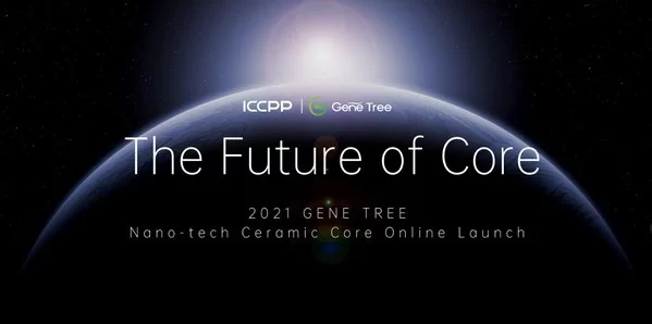
SHENZHEN, China, Sept. 18, 2021 — ICCPP, a global atomization company, has unveiled its first-ever ceramic core technology brand GENE TREE at the 2021 Nano-tech Ceramic Core Global Online Launch Conference on September 16. The release of GENE TREE marks a revolution in electric atomization R&D while also introducing a new generation of ceramic core products into the industry.

2021 Nano-tech Ceramic Core Global Online Launch Conference

Themed "The Future of the Core", the conference emphasized the continued development and innovations of electronic atomization technology, as well as demonstrating ICCPP’s determination to shape the future of the industry. Its new GENE TREE nano-tech ceramic core products promise to improve the efficiency and stability of atomization and increase product lifespan.

"GENE TREE is the culmination of countless hours of R&D and almost a decade of experience in electric atomization technology. We are thrilled to launch our breakthrough research achievement with the international community and usher in the future of ceramic cores," said ICCPP CEO EVEREST Zhao.

ICCPP has established a 300-strong R&D team. GENE TREE nano-tech ceramic core products were realized by this team after over 1,000 days spent on repeating technical explorations and scientific experiments and tens of thousands of hours spent refining one thousand sets of ceramic core material formulations. In addition, the R&D team overcame a series of technical production challenges to ensure mass-produced ceramic cores were at a world-class level in terms of resistance consistency and appearance.

GENE TREE Ceramic Cores

With the "powder-free" concept, GENE TREE products harness raw materials made from new environmentally-friendly mineral materials, which migrate and diffuse into the three-dimensional network ceramic skeleton at a high temperature. Following this, the grain micro-structure is rebuilt and the multi-phase co-existence structure improves the ceramic toughness. Meanwhile, dispersion is distributed in the three-dimensional ceramic skeleton to form a lipophilic matrix layer, which can improve the lipophilicity and oil storage of porous ceramic. Atomization tests have demonstrated that the temperature of the ceramic heating surface and atomization remains stable between four to 11 watts.

Unlike other products, GENE TREE’s safe operation power range can also be raised from 8 watts to 11 watts to fully meet the requirements of different products. The heating film remains stable in temperature and the GENE TREE supports continuous atomization for 4000 seconds — increasing its lifespan by five times compared with other mainstream products.

As ICCPP’s first ceramic core product, GENE TREE has garnered widespread attention from the industry since its launch. With plans to ramp up production capacity and sales for B2B clients, GENE TREE has established itself as a key player straight out of the gate, as well as the leader in electric atomization technology.

About ICCPP

ICCPP is a global technology group with nearly a decade of experience in technology research and development, product design, manufacturing, brand building and other fields. Its products and services are distributed in more than 70 countries and regions, with approximately 30 million users.

Tingkai Xu
kai@voopootech.com
+86-15957944779

Evo successfully responds to e-commerce growth with Kӧrber and Locus Robotics


Sports retailer increases picking speed by 157% by deploying AMRs in just 53 days

HAMBURG, Germany and WILMINGTON, Mass., Sept. 10, 2021 — Körber and long-time strategic partner Locus Robotics, the global leader in warehouse robotics, together are enabling evo to dramatically improve ecommerce order fulfillment and productivity by deploying Locus’s autonomous mobile robot (AMR) solution alongside Kӧrber’s warehouse management system (WMS).

A LocusBot assisting one of evo's warehouse workers.
A LocusBot assisting one of evo’s warehouse workers.

"The automation solution from Locus Robotics and Körber was one of the first technologies that I have seen come into the warehouse where the team was excited from the get-go," said Chris Christiansen, Outbound Manager, evo. "The improvement of speed and efficiency is impressive, allowing us to boost productivity and efficiency ahead of the 2020 holiday season while keeping our workers safe amid COVID-19 concerns. We are also well equipped with the flexibility to scale up and down on a Robots-as-a-Service (RaaS) principle."

Throughout the COVID-19 pandemic, evo faced serious challenges navigating rapid growth in demand at their warehouse as well as peak seasons – pushing the company to the limits of its capacity. Due to hard-to-find temporary and seasonal workers, as well as a desire for improved productivity in its fulfillment operations, evo specifically struggled to keep up with e-commerce orders. Additionally, evo had to consider COVID-related safety and social distancing guidelines while designing their work processes.

evo turned to Körber, their trusted supply chain partner since 2014. Körber had already delivered the warehouse management system (WMS) and would now provide a multi-bot warehouse automation solution with Locus that allowed the required flexibility and efficiency.

Körber and Locus implemented the AMR solution in just 53 days. This allowed evo to be ready to meet and exceed growing order volumes with zero downtime or disruption. The project started with ten robots that move independently through the warehouse, collaboratively supporting pickers by eliminating unproductive walking time and physical labor. Further, the visual imaging of the product to be picked helped accelerate pick rates.  To support peak season, evo added seven additional robots for expected higher volumes at the facility, using Locus’s innovative RaaS model. This is managed via Kӧrber’s WMS.

The deployment has resulted in a significant increase to workers’ picking speeds up from an average of 35 units per hour (UPH) with manual carts to 90 UPH with LocusBots. Some workers topped 125 UPH, an increase of more than 157 percent.

Rick Faulk, Chief Executive Officer, Locus Robotics, adds: "We are proud to partner with Körber to deploy our powerful and efficient multi-bot solution to support evo’s warehouse operations. Our purpose-built robotics solution has seamlessly addressed the needs of evo’s high-growth warehouse, now and into the future. We look forward to continuing to work with them to drive operational efficiencies and growth."

"The supply chain industry is dealing with multiple challenges, especially in times of disruption," says Bill Ryan, CEO Software North America, Körber Business Area Supply Chain. "In today’s world with increasing complexity, we’re looking to technology to solve these problems. With the new AMR solution which we were able to deploy with our partner in record time, evo is able to increase performance while providing a safe and smart working environment for the staff."

About evo

evo is an innovative action sports and outdoor lifestyle retailer with roots in the Pacific Northwest. The company’s focus on community and crafting extraordinary customer experiences has propelled it from its humble beginnings in a small Seattle apartment to one of the fastest-growing lifestyle retailers in the nation. evo has grown from its strong online presence to open flagship stores in Seattle, Portland and Denver, continuing with the extension of its global reach into Whistler, BC. All locations proudly showcase evo’s trademark blend of sport, culture, art, retail and service. Through evoTrip, customers can experience the evo lifestyle of sport and culture through destination travel to ski, snowboard, surf, or mountain bike remote wonders around the world. Leveraging our success to give back, evo helps underserved youth through volunteer time, donations and other support for local and national non-profit organizations including Big Brothers Big Sisters, SOS Outreach and Chill Foundation.

About Locus Robotics

Locus Robotics’ revolutionary, multi-bot solution incorporates powerful and intelligent autonomous mobile robots that operate collaboratively with human workers to dramatically improve piece-handling productivity 2X-3X, using less labor than traditional picking systems. This award-winning solution helps retailers, 3PLs, and specialty warehouses optimize labor to efficiently meet and exceed the increasingly complex and demanding requirements of fulfillment environments. Locus robots may be integrated easily into existing warehouse infrastructures as well as new warehouses without disrupting workflows, instantly transforming productivity without transforming the warehouse. www.locusrobotics.com.

About the Körber Business Area Supply Chain

Supply chains are growing more complex by the day. Körber uniquely provides a broad range of proven, end-to-end supply chain solutions fitting any business size, strategy or appetite for growth. Capable of delivering software, automation, voice, robotics, and materials handling – plus the expertise to tie it all together. We are a global partner not just for today, but also as the needs of supply chains continue to evolve. Conquer supply chain complexity – with Körber. The Business Area Supply Chain is part of the global technology group Körber. Find out more on www.koerber-supplychain.com   

Contact:

Heather Smith 
Director Corporate Communications  
Körber Supply Chain 
Heather.smith@koerber-supplychain.com 
T +1 800 3283271

Photo – https://techent.tv/wp-content/uploads/2021/09/evo-successfully-responds-to-e-commerce-growth-with-kd3a7rber-and-locus-robotics.jpg 
Logo – https://techent.tv/wp-content/uploads/2021/09/evo-successfully-responds-to-e-commerce-growth-with-kd3a7rber-and-locus-robotics-2.jpg

Related Links :

https://www.koerber-logistics.com/en/home.html

Revolutionary X-ray Technology From Australia to Transform American Airport Security

SeaTac chosen for Micro-X Inc’s USA headquarters
Official Opening at 10 am PDT, Friday May 28
855 S 192nd Street, Suite B600, Seattle, WA 98148

With:

  • Congressman Adam Smith, chair of the House Armed Services Committee
  • Brigadier Hugh Meggitt representing Australian Defence Staff, Embassy of Australia
  • Stephen Patterson, South Australian Minister for Trade and Investment (Pre-recorded)
  • Erin Sitterley, SeaTac Mayor

Technology featured:

  • World’s first electronic x-ray tube, using nano technology to create the most significant innovation in x-ray tubes in over 100 years
  • Rover: the first FDA approved system using Micro-X’s revolutionary x-ray technology
  • Prototype self-service baggage scanner, reimagining the future of airport security.

SEATTLE, Wash., May 28, 2021 — Australian company, Micro-X has chosen SeaTac, Washington State, as its US headquarters as it expands its capabilities to better support their rapidly growing business.

The proximity to the Airport for Micro-X’s future airline passenger self-screening development, the exceptional level of software talent in the greater Seattle Region, and the room in south King County for the company’s expansion plans all contributed to SeaTac being chosen as the ideal location.

Micro-X has reinvented how X-rays are generated. Using their patented carbon nanotube X-ray cold emitter technology, they’ve invented Rover, a mobile X-ray machine that weighs less than 220 lbs and is ruggedized for high intensity use in field hospitals and remote locations.

But the technology can do much more. It could transform airport security across America, enabling faster and more reliable X-ray baggage screening, reimagining airport checkpoints.

"Today, we’re expanding our US operations," says Peter Rowland, Micro-X Australian CEO.

"Our new SeaTac facility will be a center of excellence for imaging product development that will revolutionize medical, defense, and security x-ray imaging," says Brian Gonzales CEO of Micro-X’s rapidly expanding US operations.

"Our mobile X-ray machines are available now for use in public and military hospitals. They’re lighter, cheaper, more robust, and more precise than our competitors."

The patented invention that makes all these ideas possible is inside our 3.3 lb x-ray tube which replaces a conventional x-ray tube weighing more than 44 lbs.

Read the full media release at https://micro-x.com/revolutionary-x-ray-technology-from-australia-to-transform-american-hospitals-and-airports/ 

Related Links :

https://micro-x.com/

“I Love Being Pioneer”– Interview with Prominent WPI-MANA Researcher

TSUKUBA, Japan, Aug. 28, 2020 — The International Center for Materials Nanoarchitectonics (WPI-MANA), a unit of the National Institute for Materials Science (NIMS), welcomed Honorary Professor Hideo Hosono of Tokyo Institute of Technology as a NIMS Distinguished Fellow and the leader of the Electro-Active Materials Team.

(Photo: https://kyodonewsprwire.jp/prwfile/release/M105739/202008183234/_prw_PI1fl_es00fXV1.jpg)

Prof. Hosono, the world-renowned researcher, is famous for creating amorphous oxide semiconductor IGZO-TFTs and room temperature-stable electrides, and discovering iron-based superconductors. He discusses his life and work in an interview.

Q: You have done important work in a variety of fields. What’s your secret?

"I don’t have any secrets. I’ve just been focusing on what I want to do without restrictions on the technical or academic field. For example, chemistry and physics as two separate disciplines have little meaning in materials science. My main interest is in functional materials utilizing electrons in solids. In the case of semiconductors, I study the movement of electrons under an electric field, and superconductors are similar–you manipulate electrons in catalysis to react with molecules on a surface.

"My PhD thesis was on line shape analysis of electron spin resonance spectra in glass–rather fundamental work. After that, I did joint work in the material sciences department at Nagoya Institute of Technology, where I worked with ceramics, especially photoactive glasses and protonic conduction in glass. I did ion implantation into SiO2 glass for a year at Vanderbilt University in the U.S. as well as research at Oak Ridge National Lab, in Tennessee.

"I returned to Japan, to Tokyo Tech, and changed my research topic from photoactive glasses to oxide semiconductors. The most visible result of my work at that time was the proposal of transparent amorphous oxide semiconductors for thin film transistors, leading to the IGZO TFT, which is now used in high-resolution LCD panels such as tablets and OLEDs for TV screens. When I started this research in 1993, there was almost no work being done in the field. But now, 25 years later, oxide semiconductors are the world standard for TFTs for flat-panel displays and beyond. It was during this work on oxide semiconductors that we discovered iron-based superconductors."

Welcome to NETX – Global Conglomerate Bellagraph Nova Group Launches Latest Technolgy Platform Focusing on AI + Robotics + Healthcare

PARIS, July 10, 2020 — Headquartered in Paris, France, the Bellagraph Nova Group (BN Group), the multi-national conglomerate overseeing 31 business entities across 100 countries is the world’s fastest growing 360 degree lifestyle platform. 

The BN Group is proud to announce its latest project to its ever-increasing portfolio: NETX, an exciting new division focused on the development and application of robotics and Artificial Intelligence (AI) technology. 

In December 2019, the three founders of the BN Group, Terence Loh, Nelson Loh, and Evangeline Shen hosted a closed door discussion session with Barack Obama, the 44th President of the United States of America to discuss their views on how technology will bring about the next industrial revolution. The three founders passionately shared their vision where technological disruption is essential to bringing about positive change in our society. As a result of their historic meeting with Barack Obama, NETX was born … The rest as they say is history.

(L-R) Bellagraph Co-Founders Nelson Loh, Evangeline Shen, President Barack Obama and Terence Loh having an engaging discussion on how the BN Group wants to harness technology to benefit mankind

In President Obama’s own words, ” What we’re seeing here is the way that technology is changing not just how you do business, not just how you buy products, but also how you interact, how you organize politically, how you get involved in the community and how you solve problems. And all of that can support millions of new jobs.”

Those very own words of President Obama prompted the three founders’ subsequent quote: “Following our meeting with President Obama in Dec 2019, the three of us were greatly inspired by his vision. It resonated strongly with ours, so much so our exhilarated actions led to the launch of NETX.” Over the last 6 months, it has been a primary focal point of the BN Group to channel its energy and global resources into the development and commercialization of the rapidly growing global robotics market which is forecast to grow to over US$160 billion by 2025. Especially in light of the post COVID-19 pandemic, the global adoption of AI and robotics will be even faster and across all aspects of our lives.

During the COVID-19 pandemic, NETX already dispatched domestic service robots to support frontline healthcare workers worldwide, protecting over 80,000 patients and medical staff. NETX has also implemented AI in its Remote Access technology which has greatly reduced the risk of exposure in otherwise hazardous conditions. In seeing the successful applications of NETX’s robotics and AI technology, the BN Group is planning the distribution and implementation of NETX to the company’s worldwide network of hospitals, clinics, commercial and retail locations.

While many questions still remain unanswered regarding the world of robotics and how these machines will affect society, there should be no question of the Bellagraph Nova Group’s unwavering commitment to simply making our world a better place by investing in the future with its focus on the development and application of robotic technology in its latest exciting chapter, NETX.

ABOUT BELLAGRAPH NOVA GROUP

Sustainability, diversity and ethics, constitute the cornerstone of BN Group’s model and compliance policy for its executives, employees and stakeholders. Our emblem is the butterfly, the symbol par excellence of endurance and perennial metamorphosis.

The Group is headquartered in the famous 10 Place Vendôme in Paris, France. With 31 entities in over 100 countries, the combined US$12 billion revenue Bellagraph Nova Group is the world’s fastest growing 360 degree lifestyle platform.

Photo – https://photos.prnasia.com/prnh/20200710/2854757-1?lang=0
Logo – https://photos.prnasia.com/prnh/20200707/2850183-1logo?lang=0

KT and Hyundai Accelerate Digital Transformation with Smart Robots

SEOUL, South Korea, June 18, 2020 /PRNewswire/ — KT Corp. (KRX: 030200; NYSE: KT), South Korea’s largest telecommunications company, announced it signed strategic cooperation and investment contracts with Hyundai Robotics, to speed up collaboration for digital transformation based on 5G, artificial intelligence (AI) and smart factory.
After KT and Hyundai Robotics contracts to speed up collaboration for digital transformation based on 5G, AI and smart factory, KT president Ku Hyeonmo and Hyundai Heavy Industries Holdings Senior Executive Vice President (SEVP) Chung Kisun are taking photo at the signing ceremony.

Under the contracts, KT will acquire a 10 percent equity stake in Hyundai Robotics, the leader in the Korean industrial robotics market, for 50 billion won.

KT also signed a business cooperation agreement with Hyundai Heavy Industries Holdings for joint efforts toward digital transformation.

The signing ceremony, held at the KT headquarters in central Seoul, was attended by KT President Ku Hyeonmo, Hyundai Heavy Industries Holdings Senior Executive Vice President (SEVP) Chung Kisun and Hyundai Robotics CEO Seo Yoo-seong, and other senior executives.

The two sides signed a memorandum of understanding in May 2019 and the new contracts solidify their ongoing collaboration to spread digital transformation based on 5G, AI and smart factory. They intend to quicken joint development of intelligent service robots, technological research in autonomous driving, and smart factory solutions.

“In the post-COVID 19 era, KT is prepared to contribute to strengthening the Republic of Korea’s industrial competitiveness and the transformation of our nation’s manufacturing industry, taking advantage of our 5G and AI capability in cooperation with Hyundai Heavy Industries Group,” said KT President Ku. “Beginning with Hyundai Heavy Industries Group, we will do our utmost to expand digital transformation in diverse areas.”

KT will undertake software development and applications related to intelligent service robots and autonomous driving, while Hyundai Robotics will be responsible for hardware development and manufacturing. This is expected to lead to the introduction of intelligent robots that not only provide hotel amenities but also serve food and beverages at restaurants, and cleaning patrol robots loaded with cleaning and security functions. For entry into the service robot market, the two parties also plan to develop collaborative robots for small factories and large franchise stores.

For a smart factory, KT will provide communication technology, cloud, ICT solutions, and related bundle products, while Hyundai Robotics will supply robots and relevant solutions. In particular, the combination of KT’s smart factory solutions, dubbed “5G Factory Makers,” and Hyundai Robotics’ Hyundai Robot Management System (HRMS) is expected to heighten smart factory process analysis, production management and predictive maintenance. The toolkits of both sides will also be applied jointly for smart hospitals and logistics.

Along with its equity participation in Hyundai Robotics, KT will seek an exchange of human resources to help refine elevation of Hyundai Robotics’ competitiveness in robotics and smart factory.

“Beyond mere production, the competitiveness of manufacturers will be determined in the future by the ability of individual businesses to read market trends and transform themselves.” said Chung Kisun, Senior Executive Vice President (SEVP) of Hyundai Heavy Industries Holdings. “Through expansive business cooperation with KT, we believe that not only Hyundai Robotics but the entire Hyundai Heavy Industries Group will be able to achieve digital transformation and thereby improve our competitiveness as leading enterprises in the world.”

Hyundai Robotics, spun off from Hyundai Heavy Industries in April 2017, became a separate corporation specialized for robotics and smart solutions in May this year. It provides smart factory and smart logistics services, and has two subsidiaries – Hyundai Robotics Shanghai and Hyundai L&S (Logistics and Solutions). The company aims for an initial public offering in 2022.

In accordance with their business cooperation agreement, KT and Hyundai Heavy Industries Group will delineate details of their collaboration, particularly through a new senior committee on joint efforts in smart solutions, digital transformation, AI and ICT, as well as other business opportunities. The group will include KT President Ku and Hyundai Heavy Industries Holdings Senior Executive Vice President (SEVP) Chung Kisun.

Last year November, KT and Hyundai Heavy Industries Holdings conducted a joint presentation on their 5G-based business cooperation, focusing on smart factory and smart shipbuilding. In February this year, they launched “AI One Team,” aiming to lift Korea to global leadership in AI, and two months later, KT and Hyundai Robotics introduced “N Bot,” an upgrade from KT’s second-generation GiGA Genie hotel robot in terms of both function and design, at the Novotel Ambassador Seoul Dongdaemun Hotel. It was followed by the signing with Hyundai Construction Equipment of a memorandum of understanding for “joint development and commercialization of 5G smart construction equipment and industrial vehicle platform.”

KT expects that its cooperation with Hyundai Heavy Industries Group will expand digital transformation into diverse industrial fields, eventually enhancing national competitiveness. To that end, KT is exerting corporation-wide efforts for digital transformation to help maximize efficiency and widen business opportunities of companies on the basis of its expertise in 5G network, AI, Big Data, cloud and ICT solution.

MEDIA CONTACTS

For inquiries, please contact our Global Media Relations Team at kt.gmrt@gmail.com

ABOUT KT CORPORATION (KRX: 030200; NYSE: KT)

KT Corp., Korea’s largest telecommunications service provider, reestablished in 1981 under the Telecommunications Business Act, is leading the era of innovations in the world’s most connected country. The company is leading the 4th industrial revolution with high speed wire/wireless network and new ICT technology. KT launched the world’s first nationwide commercial 5G network on April 3, 2019, after successfully showcasing the world’s first trial 5G services at the PyeongChang Winter Olympic Games in February 2018. This is another milestone in KT’s continuous efforts to deliver essential products and services as it aspires to be the number one ICT Company and People’s Company.

For more information, please visit our English website at https://corp.kt.com/eng/

Cision View original content to download multimedia:http://www.prnewswire.com/news-releases/kt-and-hyundai-accelerate-digital-transformation-with-smart-robots-301078524.html

Source: KT Corp.

ECOVACS ROBOTICS Launches the DEEBOT OZMO T8 Family Putting AI to Work For a Better Looking Home

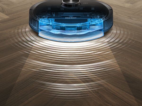
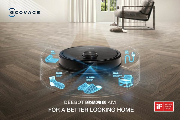
SINGAPORE, May 25, 2020 /PRNewswire/ — ECOVACS ROBOTICS launched the DEEBOT OZMO T8 family, its latest series of high-end intelligent robotic vacuum cleaner. First family member DEEBOT OZMO T8 AIVI features ECOVACS’ optimized AIVI™ (Artificial Intelligence and Visual Interpretation) Technology for faster obstacle recognition, TrueMapping™ Mapping and Navigation Technology, and OZMO Pro for advanced mopping performance. In addition, its on-demand feature Video Manager makes the DEEBOT OZMO T8 AIVI a personal and powerful housekeeping robot, bringing users advanced interaction between human and robot by enabling them to reach to a new level of robotic vacuum cleaner user experience. The new DEEBOT OZMO T8 AIVI is also the winner of the internationally respected iF Design Award of 2020.

ECOVACS DEEBOT OZMO T8 AIVI

“With over 22 years of innovative technology development, ECOVACS ROBOTICS has driven the transition from traditional methods of home cleaning care to automated home care,” said David Qian, CEO of ECOVACS ROBOTICS, “Our new DEEBOT OZMO T8 family gives consumers what they have been looking for, a high-end intelligent solution for a hassle-free cleaning experience.”

Latest Optimized AIVI™ Technology – Sophisticated Obstacle Avoidance

With the latest optimized AIVI™ Technology, the DEEBOT OZMO T8 AIVI can recognize and avoid obstacles 200% faster with a predicted 60% reduction in entanglement rate compared to existing AIVI products, relying on machine learning to adapt to the user’s unique home environment. It also intelligently suggests extra cleaning based on its record of spots avoided, to offer a more thorough cleaning performance.

The DEEBOT OZMO T8 AIVI can automatically recognize objects including shoes, charging docks, cables, cloths, and socks to avoid obstacles and prevent the robot from getting stuck.

As the industry’s most intelligent robotic vacuum cleaner, further advanced AI-powered functions will be offered via OTA (Over the Air) Technology in the coming months, including automated detection of U-shaped chairs and rugs. For U-shaped chairs, the robot will make a single attempt to pass them, and for rugs the robot will automatically adjust roller brush speed to avoid getting stuck.

First-adopt Aerospace-standard dToF Detection Technology[1] Powers Brand-new TrueMapping™ to Enable Precise and Customized Cleaning

Compared with the previous generation of Smart Navi® 3.0, the TrueMapping™ laser-based mapping and navigation technology can detect a double distance and has four-fold precision to detect objects as small as two millimeters. With the new technology, DEEBOT OZMO T8 AIVI can now scan, map, and plan an efficient cleaning path in a large house faster and more precisely.

TrueMapping™ Mapping and Navigation Technology also offers users a more customized and intelligent cleaning experience. The DEEBOT OZMO T8 AIVI has Multi-floor Mapping Technology that can scan and store multiple maps of different levels of a user’s home. For first time cleaning, the robot automatically divides the whole cleaning environment into multiple areas based on the floorplan. Once the robot has identified the appropriate map, it can customize its cleaning process to each level. Furthermore, the upgraded Virtual Boundary™ can proactively provide recommendations for virtual walls around areas where it may easily become stuck, with the user only needing to click the confirmation on the ECOVACS Home App to accept the recommendations.

ECOVACS DEEBOT OZMO T8 AIVI

A Reliable Cleaning Partner with Powerful Vacuuming and Mopping Capabilities

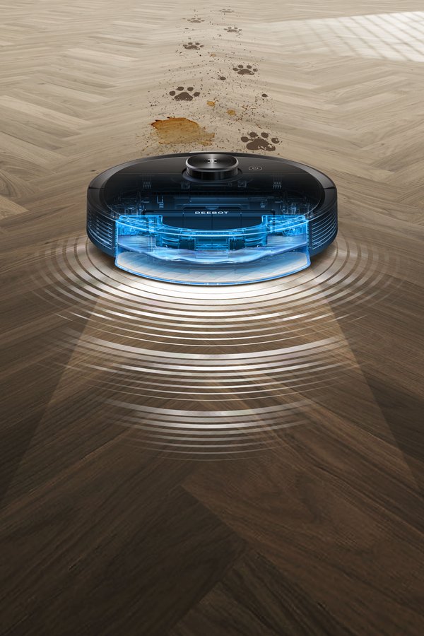
The DEEBOT OZMO T8 AIVI provides powerful vacuuming and mopping capabilities, that can both be completed in one go. The four-step cleaning offers efficient vacuuming that won’t even miss dust in 4mm deep cracks. This new family member also includes an interchangeable enhanced mopping module featuring the brand-new OZMO™ Pro Mopping System, enabling robots to deal with stubborn stains 5X efficient than human[2] by using electrically powered high-frequency vibration, and a unique fine mopping mode comparable to an electronic mop, which makes it the most powerful mopping ability in its kind[3]. Alternatively, ECOVACS’ signature mopping technology still be available with its OZMO Mopping System, featuring an electronically controlled water pump and 240 ml large water tank, ensures long-lasting mopping efficiency by tackling dirt and dried liquid to offer a smooth and consistent clean. What’s more, the OZMO™ Mopping System can remove over 99%[4] of bacteria based on the test report from a Japanese testing agency.

With a larger battery of 5200 m(A)h, DEEBOT OZMO T8 AIVI can work for three hours and clean large areas of up to 300 sqm easily. The robot’s carpet detection technology allows it to automatically increase suction power on carpets when vacuuming and avoid carpets when mopping, keeping the cleaning experience completely automated.

When paired with the ECOVACS Home App, or smart home devices such as Amazon Echo/Dot and Google Home, users can also control the robot remotely. The intuitive robot will manage its own updates adding new features and functions in the future by using OTA technology. Users can update the App to get the optimized functions.

In addition, with the real time camera acting as an on-demand video manager for the entire house, users can choose to use it for watching the home and monitoring the status of pets, children, or elders in their house anytime and anywhere through the ECOVACS Home App.

Power-up Kit

As part of the launch of the DEEBOT OZMO T8 family, another power-up kit will soon be introduced to enhance overall cleaning performance and user experience. The Auto-Empty Station which cleans the robot’s dustbin automatically after cleaning. The station’s disposable dust bag holds up to 30 days of dirt and debris to dramatically reduce the need to frequently replace the dust bag, so that users can enjoy cleaning homes for weeks without the hassle of dumping the bag.

Pricing and Availability

The DEEBOT OZMO T8 AIVI is available today on Lazada for SGD 729. For more information, please visit ecovacs.com or connect with us on Facebook [https://www.facebook.com/ecovacs.sg/]. More products from the DEEBOT OZMO T8 family will be released later this year.

[1] The First DEEBOT with dToF Laser-based Sensors

[2] Test from HQ Laboratory, 100 wipes/min by Hand-wiping, 480 wipes/min by OZMOTM Pro

[3] Test from HQ Laboratory, The Strongest Ability of Moving Stubborn Stains Away with OZMOTM Pro

[4] Certified by Hygiene & Microbiology Research Center, Japan, 2019

About ECOVACS ROBOTICS

Innovating Since Day One – Creating the Intelligent Home.

At ECOVACS ROBOTICS, we care about innovating solutions to enhance your lifestyle. Based on deep understanding of use cases and consumer experiences, we design robots that help you to “live smart, enjoy life”.

With over 20 years of design and industry-leading research, we have led the market as homes become more intelligent and responsive. We are building a world where your home asks less of your attention, becomes more seamless and powerful, and frees you to spend more time doing what you love.

Media Contact

ECOVACS ROBOTICS
APAC Marketing
Christy Chau
+852-3700-2001
Christy.chau@ecovacs.com

Photo – https://photos.prnasia.com/prnh/20200525/2812433-1-a?lang=0
Photo – https://photos.prnasia.com/prnh/20200525/2812433-1-b?lang=0